


- News
19 February 2015
Combining van der Waals technologies to make light-emitting diodes
A research team including Nobel laureates Andre Geim and Konstantin Novoselov has developed light-emitting diodes (LEDs) combining transition metal dichalcogenide (TMD) wells, hexagonal boron nitride (hBN) barriers and graphene (Gr) electrodes [F.Withers et al, Nature Materials, published online 2 February 2015].
The researchers from University of Manchester and University of Sheffield in the UK and Japan's National Institute for Materials Science used a series of 'peel and lift' processes to create various heterostructures held together by van der Waals forces (Figure 1).
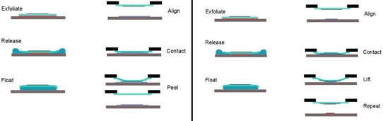
Figure 1: Schematics of peel (left) and lift (right) processes.
Peeling involves mechanical exfoliation of the source crystal layers onto a polymer double layer, dissolving the bottom polymer layer to release and float the membrane (crystal on single polymer layer), flipping and aligning with the target structure, and finally peeling off the polymer handling layer. Lifting is similar, except that the membrane is used to lift exfoliated material from a flake of crystal on a substrate for transfer to another thermally oxidized silicon wafer.
The LED structures consisted of molybdenum disulfide (MoS2, Figure 2), or tungsten disulfide/diselenide (W(S/Se)2) quantum wells separated by hBN barriers. The researchers claim 100% yield of functioning devices with strong electroluminescence "that remains unchanged after months of periodic measurements, which demonstrates the robustness of the technology and materials involved." Graphene layers were used for top and bottom electrodes in combination with chromium/gold metal contacts.
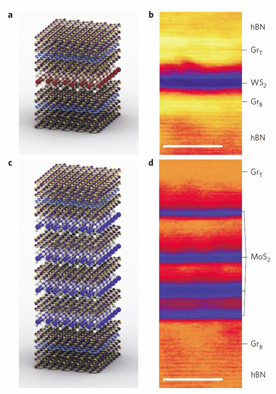
Figure 2: a, Schematic of single quantum well structure (hBN / GrB / 2hBN / Gr<span class="subscript">B</span> / 2hBN / GrT / hBN). b, Cross-sectional bright-field STEM image of single-well heterostructure. c, d, Schematic and STEM image of the multiple quantum structure (hBN / GrB / 2hBN / MoS2 / 2hBN / MoS2 / 2hBN / MoS2 / 2hBN / MoS2 / 2hBN / GrT / hBN). The number of hBN layers between MoS2 QWs in d varies from schematic. Scale bars, 5nm.
The heterostructures were analyzed by electroluminescence and photoluminescence under various biases, along with electron microscopy and energy-dispersive x-ray spectroscopy.
Under electroluminescence (EL), the researchers estimated that a single quantum well of MoS2 achieved an external quantum efficiency (EQE) of ~1% – ten times larger than for planar pn junctions of MoS2 and 100x that of Schottky barrier (metal-semiconductor) emissions. The efficiency of photoluminescence (PL) was lower – the researchers comment: "Relatively low EQE found in PL indicates that the crystal quality itself requires improvement and that even higher EQE in EL may then be achieved." The line-width of these LEDs was as narrow as 18meV.
A device with three quantum wells of MoS2 (Si / SiO2 / hBN / GrB / 3hBN / MoS2 / 3hBN / MoS2 / 3hBN / MoS2 / 3hBN / GrT / hBN) achieved a 6% efficiency. The turn-on current density was 1.8nA/μm2 – nearly two orders of magnitude lower than for a single well. The voltage at this current injection was around 3.9V.
Four asymmetric quantum wells increased the efficiency to 8.4%. "This high QE is comparable to the efficiencies of the best modern-day organic LEDs," the researchers write.
An LED with mixed WSe2/MoS2 wells (Si / SiO2 / hBN / GrB / 3hBN / WSe2 / 3hBN / MoS2 / 3hBN / GrT / hBN) had a QE of ~5%, an order of magnitude stronger than for the single well. The researchers suggest that this could be due to charge transfer to the well with the smallest energy gap after electron-hole generation in both wells.
The peak performance for the devices was at very low temperature, below 150K. At room temperature, the efficiency was around a factor of two or three lower. A single-well device assembled on a flexible polymer substrate (PET) was able to withstand bending up to 1% uniaxial strain without change in the EL spectrum.
The researchers hope that the application of chemical vapor deposition (CVD) to the preparation of such heterostructures will allow scaling up of production, as needed for commercial mass applications.
LEDs Metal dichalcogenide wells Hexagonal boron nitride barriers Graphene electrodes
http://dx.doi.org/10.1038/nmat4205
The author Mike Cooke is a freelance technology journalist who has worked in the semiconductor and advanced technology sectors since 1997.


