


- News
23 December 2015
imec presents record-breaking indium gallium arsenide transistors on silicon
The imec research center in Belgium claims record results for indium gallium arsenide (InGaAs) gate-all-around (GAA)-channel devices on 300mm silicon wafers. The researchers from imec, ASM, Poongsan Inc and Belgium's KU Leuven reported their achievements at the International Electron Device Meeting (IEDM) in Washington DC [Session 31.1, 9 December 2015]. An imec-only team also reported on InGaAs homojunction tunnel field-effect transistors (TFETs) with claimed superior subthreshold swing (SS) reliability compared with metal-oxide-semiconductor FETs (MOSFETs) [Session 31.7, 9 December 2015].
The peak transconductance (gm) for the GAA transistors was as high as 2200μS/μm for the 50nm gate-length GAA channel device, while the subthreshold swing (SSSAT) was as low as 110mV/decade. The drain bias was 0.5V.
The GAA structure (Figure 1) was achieved through fin replacement and a replacement metal gate (RMG) process flow. ASM supplied a newly developed interlayer material for the gate stack, which was applied using atomic layer deposition (ALD). The researchers also added a high-pressure 400°C annealing step to increase gm by 22%. The team focused on improving the channel epitaxy process quality along with passivation of the gate-to-channel interfaces.
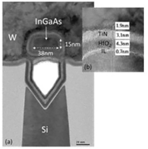 Figure 1: Transmission electron micrograph (TEM) of complete GAA InGaAs nanowire FET and high-resolution TEM (HRTEM) of gate stack.
The ASM interlayer material was combined with hafnium dioxide gate insulator. The researchers compared devices using the ASM material with GAA transistors that implemented a more traditional aluminium oxide layer. The novel interlayer stack achieved 2.2x higher gm, compared with the reference aluminium oxide stack.
The TFETs used InGaAs with the indium content increased to 70%, compared with the 53% often used in III-V devices. The increased indium content boosted the performance of 8nm-channel TFETs, giving a claimed record on-current of 4μA/μm, with an off-current of 100pA/μm, and a minimum SS of 60mV/decade at room temperature (300K). The operating voltage (Vdd) was 0.5V with 0.3V drain. Reliability assessment showed that the minimum SS and gm were more immune to positive-bias temperature instability (PBTI) stress than equivalent MOSFETs.
imec sees TFETs as potential technologies beyond present and near-future FinFETs and GAA-nanowire devices for sub-0.5V operation. By studying the impact of defects and optimizing the channel structure, imec hopes to pave the way to advanced logic devices based on III-V-on-Si for high-performance or ultra-low-power applications.
Aaron Thean, vice president & director of imec's advanced logic R&D program, comments: "Imec's R&D enables Moore's law beyond the 5nm technology node through three approaches. First, we are tackling the technology challenges to extend silicon CMOS devices towards smaller nodes. At the same time, we research into disruptive heterogeneous solutions for beyond-silicon CMOS devices to increase performance and introduce new functionalities. Lastly, imec pursues emerging beyond-CMOS devices and systems such as spintronics to investigate further functional scaling beyond device-density-driven scaling."
imec works on these projects in conjunction with key partners in its core CMOS programs such as GlobalFoundries, Intel, Micron, Panasonic, Qualcomm, Samsung, SK Hynix, Sony and TSMC.
The author Mike Cooke is a freelance technology journalist who has worked in the semiconductor and advanced technology sectors since 1997.


