


- News
28 December 2015
Toward quantum computing on silicon-on-insulator platform
Researchers in France believe they have made preliminary steps towards establishing a silicon-on-insulator (SOI) complementary metal-oxide-semiconductor (CMOS) platform for quantum information processing. Quantum information processing promises a revolution in cryptography and database searching. In particular, the superposition of quantum amplitudes enables a radical form of parallel processing for which a large number of potential super-efficient algorithms have been developed (and implemented on a relatively small scale in various model/prototype systems).
CEA-Leti and CEA-Inac have adapted a quantum dot technology originally developed for very-large-scale integration (VLSI) CMOS circuits. The dots are located beneath the gate electrode of field-effect transistors [Romain Lavieville et al, Nano Letters, vol15, p2958, 2015]. The dots can be populated with a small number of charge carriers (electrons or holes, depending on nFET or pFET structure), when the operating temperature is 0.1K.
Control circuitry accesses the quantum dot FETs through SOI nanowire FETs developed at Leti. Together, Leti and Inac have demonstrated the co-integration and operation of quantum objects with conventional CMOS control circuitry in the form of standard ring oscillators. The devices were produced on 300mm SOI substrates.
Louis Hutin at Leti reports: "This technology has acquired a certain degree of robustness, and we aim at using it with very minor modifications to demonstrate qubits co-integrated with their control electronics. This co-integration success represents a critical asset for the eventual design of a quantum computer."
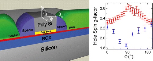
Figure 1: Schematic and plot of device with highly anisotropic and gate-dependent magneto-transport of holes as indicated by g-factor. The researchers believe that these characteristics could enable electrically driven g-tensor-modulation spin resonance with Rabi frequencies of several hundred megahertz.
Since quantum bits (qubits) are generally encoded on spin states, the researchers have been exploring different manipulation and read-out schemes. Some of the research has used radio-frequency signals to access single-charge events, including spin states in some cases. Another approach (Figure 1) has explored electrical driving of the spin with high-frequency modulation of a p-FET gate [B. Voisin et al, Nano Letters, published online 24 November 2015].
Electrical control and read-out of spin states would allow faster and more localized action compared with more traditional magnetic field approaches. Also, the use of a semiconductor system rather than atomic trapping or superconducting devices should allow much easier upscaling of complexity.
This is true in particular for silicon-based devices as opposed to approaches based on III-V compound semiconductors. Silicon spintronic development has been enabled by the use of isotopically pure silicon-28, which avoids decoherence of quantum spin states through coupling with nuclear spins. The silicon-28 nucleus is the most common isotope and is spin-free/zero. The nuclear spins of III-V semiconductors limits the lifetime of quantum spin states in electron and hole carriers.
The team believes that actual qubit demonstrations in their CMOS SOI device structures could be close, and after that would come near- and long-range coupling of multiple qubits.
Leti and Inac are involved through CEA in the Silicon platform for Quantum Spintronics (SiSPIN) European Union (EU) Seventh Framework Programme, along with TU Delft, IBM Zurich, University of Copenhagen, University of Basel, and University of Linz. The SiSPIN collaboration is exploring technological implications ranging from improved switching performance of classical logic gates (e.g. towards lower energy consumption) up to implementation of quantum computing based on spin qubits.
Quantum dot field-effect transistors Quantum computing SOI CMOS
http://inac.cea.fr/en/index.php
http://pubs.acs.org/doi/abs/10.1021/acs.nanolett.5b02920
The author Mike Cooke is a freelance technology journalist who has worked in the semiconductor and advanced technology sectors since 1997.


