


- News
15 December 2015
Single-crystal gallium arsenide on quasi-nominal silicon
Université Grenoble Alpes in France and Applied Materials in the USA have been developing techniques to grow gallium arsenide (GaAs) on silicon substrates with a small offcut angle [Y. Bogumilowicz et al, Appl. Phys. Lett., vol107, p212105, 2015]. The researchers label such substrates 'quasi-nominal', in comparison with the much larger offcut angles often used in attempts to grow GaAs on silicon.
The researchers comment: "We have found that small offcut variations greatly influence how GaAs grows on Ge-buffered silicon substrates and that the offcut angle that yields single domain layers in MOVPE can be as low as 0.5° instead of the 4°–6° angle typically found in the literature."
The small 'quasi-nominal' offcut angle makes the process more compatible with existing silicon manufacturing technology and also eliminates the need for elaborate high-temperature silicon wafer preparation. The aim of such research is to make the high-mobility and direct-bandgap properties of III-V materials available for close integration into silicon electronics. High mobility enables higher-speed signal processing and a direct bandgap creates opportunities for the efficient generation and capture of light.
In order to bridge the 4% lattice mismatch between the materials, the researchers first applied a thick layer of germanium. There is also a thermal expansion mismatch, which can lead to cracking when the processed wafer cools.
An additional problem can arise with polar materials such as GaAs being grown on non-polar silicon where different 'anti-phase' domains are created with different gallium/arsenide layer sequences. Large offcut angles to give double atomic steps on the growth substrate surface is one way to deal with this. Another technique is to begin growth with an arsenic-only layer and then introduce the gallium source.
The researchers performed metal-organic vapor phase epitaxy (MOVPE) on 300mm (001) silicon wafers. The source precursors were trimethylgallium (TMGa) and tertiarybutylarsine (TBAs) in hydrogen carrier gas.
The substrate was 775μm thick with small offcut angle (less than or equal to 0.5°) in the <110> crystal direction. The researchers comment: "In our case, this small offcut was intentional, but in practice, nominal (001) substrates are always slightly mis-oriented, whether intentional or not."
The substrate was prepared with a 1μm layer of germanium as a strain relaxed buffer. This layer was grown in a separate epitaxial tool specifically used for group IV elements. The source was germane (GeH4). The deposition temperature was varied in two low/high-temperature steps (400°C/650°C). The process also included thermal cycling in hydrogen between 650°C and 850°C with the aim of minimizing the generation of threading dislocations to densities of the order 107/cm2. The germanium layer exhibited root-mean-square roughness of less than 1nm on a 5μmx5μm field.
Applied's Siconi etch process was used to remove oxide residues after a wet etch designed to shift native oxide. The Siconi dry process was performed in-situ in the MOVPE reaction chamber before GaAs deposition, which consisted of a 700°C hydrogen bake and GaAs growth between 500°C and 700°C.
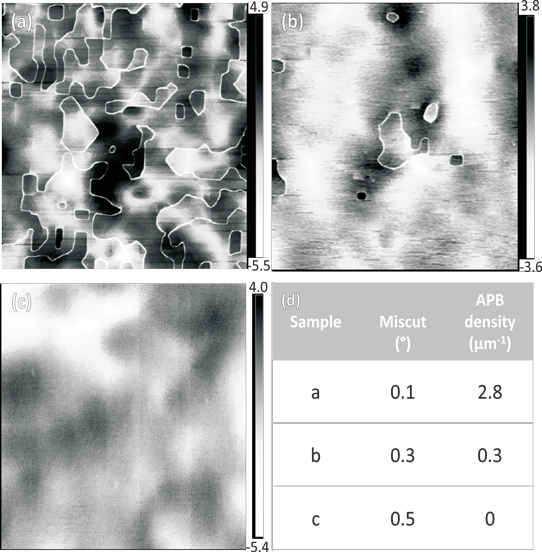
Figure 1: 5μmx5μm AFM images of surface of GaAs layers grown on Ge-buffered silicon (001) substrates with three different offcut angles: (a) 0.1°, (b) 0.3° and (c) 0.5°. Scales are labeled in nanometers. Table (d) presents APB density measured for each sample. AFM image sides are along <100> directions.
X-ray diffraction analysis showed the Ge and GaAs layers to be single crystal. The Ge and GaAs layers were tensile strained. The degree of strain relaxation was 104% and 106% for the Ge and GaAs layers, respectively. The analysis also suggested that the crystal quality improved for higher offcut angles (Figure 1).
The anti-phase boundary density was assessed using atomic force microscopy (AFM). The length of APB lines per unit area gave a per micron result. The 0.5° offcut sample had zero APBs. The threading dislocation density in the GaAs layer was between 5x10⁷/cm2 and 1x10⁸/cm2.
The researchers believe that avoiding APBs requires a distance between atomic steps to be less than a threshold value and control of the growth process to annihilate APBs that are inevitably generated initially. The atomic stepping is controlled by the offcut angle.
GaAs GaAs on silicon substrates MOVPE
http://dx.doi.org/10.1063/1.4935943
The author Mike Cooke is a freelance technology journalist who has worked in the semiconductor and advanced technology sectors since 1997.


