


- News
31 August 2015
Plasma pre-treatment for gallium nitride chemical mechanical polishing
Osaka University in Japan has developed a plasma pre-treatment for chemical mechanical polishing (CMP) on gallium nitride (GaN) that avoids creating enlarged etch pits [Hui Deng et al, Appl. Phys. Lett., vol107, p051602, 2015].
Surface atomic structure, roughness and sub-surface damage can adversely impact electronic performance. CMP is widely used to create atomic-level flatness in microelectronics. However, wide-bandgap materials – such as GaN, diamond, and silicon carbide – tend to be much harder than the mainstream electronic material of silicon for which CMP was developed.
A further problem for GaN CMP is that it is usually grown on foreign substrates such as sapphire, silicon carbide, or silicon. Lattice and thermal expansion mismatching between GaN and the substrate leads to crystal defects. Etching or CMP tends to preferentially remove material around dislocations, giving etch pits. Indeed, the density of etch pits is a common measure of the dislocation density of GaN.
The process was performed on commercial substrates with an 8μm undoped GaN epilayer on 2-inch sapphire.
The CMP was performed with 2000 rotations per minute and 3.74kPa pressure on the suede-type polishing pad from FILWEL Co Ltd (NP178). Two types of commercial slurry were tested – one containing silica (SiO2) and the other ceria (CeO2).
The plasma for the 30-minute pre-treatment (Figure 1) consisted of carbon tetrafluoride in helium carrier gas at atmospheric pressure. The distance between the plasma generation electrode and the GaN surface was 1.6mm. The electrode was 3mm in diameter.
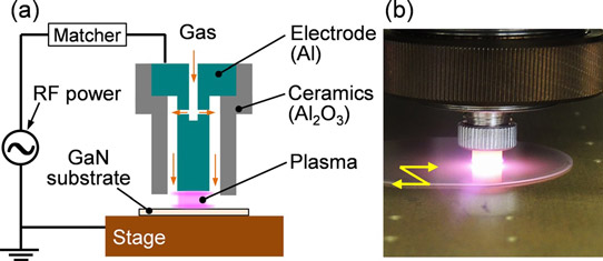
Figure 1: (a) Schematic of experimental setup for plasma irradiation. (b) Image of atmospheric-pressure CF4 plasma.
The action of the 18W 13.56MHz radio-frequency radiation was to dissociate fluorine radicals from the reactive part of the gas. Such radicals are known to react with GaN. X-ray photoelectron spectroscopy (XPS) found that the modified layer consisted of GaF3. This layer was about 30nm thick, according to cross-sectional transmission electron microscopy (XTEM).
Without the pre-treatment, the CMP with either slurry resulted in enlarged pits at dislocation sites. The effect was particularly bad for silica slurry.
The researchers only applied ceria slurry in the CMP tests on pre-treated material, since it was found to give better results on untreated GaN. After 8 minutes the protection layer was removed, but no enlarged pits were formed around the dislocations ('just-polished'). Continuing the CMP beyond this ('over-polished') created enlarged pits. Performing CMP for shorter than 8 minutes resulted in some of the GaF3 protection layer remaining on the substrate ('under-polished').
The 8-minute CMP resulted in peak-to-valley surface roughness of 1.00nm (Figure 2). The root-mean-square roughness was 0.11nm.
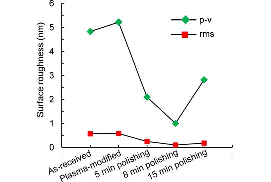
Figure 2: Change in surface roughness of GaN processed by plasma irradiation and CMP.
The researchers expect high device performance in their future work from the combination of plasma pre-treatment and time-controlled CMP.
http://dx.doi.org/10.1063/1.4928195
The author Mike Cooke is a freelance technology journalist who has worked in the semiconductor and advanced technology sectors since 1997.


