


- News
27 August 2015
LayTec metrology speeds up process development on 100mm semi-polar (11-22) GaN on r-plane PSS
At the 17th US Biennial Workshop on Organometallic Vapor Phase Epitaxy (OMVPE-17) in BigSky, Montana, USA (2-7 August), Dr Frank Brunner of FBH (Ferdinand-Braun-Institut für Höchstfrequenztechnik) of Berlin, Germany presented his latest results on the growth of semi-polar (11-22)-oriented gallium nitride (GaN) on r-plane patterned sapphire substrate (r-PSS) in an Aixtron AIX 2600G3-HT metal-organic chemical vapour deposition (MOCVD) reactor (in 8x4"-wafer confiuration).
In his talk 'Large area heteroepitaxial (11-22) - GaN growth', Brunner underlined that cost-efficient growth process optimization for these semi-polar GaN structures on 100mm PSS substrates would not have been possible without comprehensive in-situ metrology. Hence, an EpiCurve TT (for reflectance and wafer bow sensing) and a Pyro 400 (for GaN temperature control) from in-situ metrology system maker LayTec AG of Berlin, Germany were used together by utilizing the two viewports of the (modified) AIX 2600G3-HT reactor top-plate.
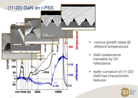
Picture: Growth of (11-22) GaN on r-PSS and related in-situ data (F. Brunner et al).
The figure shows how all details of the highly complex growth mode show up in the combined reflectance, wafer bow and temperature data.
LayTec Metrology FBH Aixtron MOCVD GaN
www.crystalgrowth.org/ACCGE-20---OMVPE-17-Conference.html
www.laytec.de/cn/solutions/advanced-rd


