


- News
3 April 2015
Indium tin oxide cladding for semi-polar InGaN laser diodes
University of California Santa Barbara (UCSB) has used indium tin oxide (ITO) as part of the cladding for semi-polar indium gallium nitride (InGaN) laser diodes (LDs) [A. Pourhashemi et al, Appl. Phys. Lett., vol106, p111105, 2015].
The semi-polar (20-2-1) crystal orientation avoids quantum-confined Stark effects (QCSEs) from the large electric fields in the (0001) c-direction that arise from charge polarization of the III-nitride chemical bond. Devices grown on c-plane material suffer from reduced efficiency because these QCSE fields tend to pull apart electrons and holes, inhibiting recombination into photons.
The ITO cladding was used to reduce the aluminium gallium nitride (AlGaN) content of the device structure. Devices with AlGaN cladding suffer from catastrophic optical mirror damage (COMD) at lower current densities due to the confined optical mode energy density.
Aluminium-free devices grown on gallium arsenide (GaAs) substrates "are less prone to both sudden failure and gradual degradation", according to the researchers. They add: "Although analogous reliability studies still need to be done for III-nitride LDs, these studies suggest that either reducing or eliminating the Al content in the cladding layers could potentially improve the manufacturability and reliability of high-power semi-polar and non-polar III-nitride LDs."
Another disadvantage of AlGaN cladding is the low hole carrier density in p-AlGaN due to the poor doping capability of even the best acceptor impurity element (magnesium). Increasing Al-content further reduces hole densities. Low hole density makes for high typical resistivity in p-AlGaN (4Ω-cm, compared with 1x10⁻⁴Ω-cm for ITO). The resistivity in p-GaN is around 1Ω-cm.
The researchers see applications for InGaN LDs in white lighting, since laser diodes do not suffer from the same efficiency droop problems as light-emitting diodes (LEDs). This is because carrier concentrations in laser diodes tend to become clamped at the value at the laser threshold, rather than continuing to increase with increased current.
UCSB used metal-organic chemical vapor deposition (MOCVD) on semi-polar (20-2-1) GaN substrates to produce the epitaxial material for the laser diodes (Figure 1). The 60nm upper and lower waveguides consisted of In0.06Ga0.94N. The 17nm electron-blocking layer (EBL) used magnesium-doped p-Al0.15Ga0.85N. The ohmic p++-GaN contact layer was 12nm thick. The magnesium doping was reduced as much as possible to avoid phonon-assisted absorption by acceptor-bound holes – a mechanism thought to be the single largest contributor to modal loss in III-nitride laser diodes.
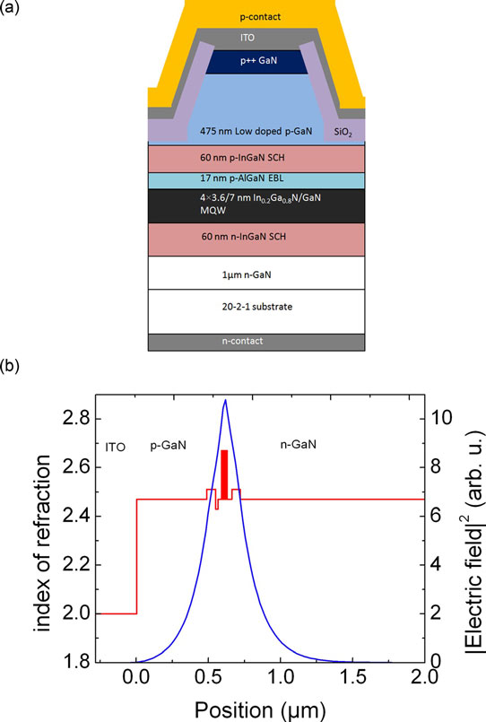
Figure 1: Schematic for laser diode (a) and calculated 1D transverse mode profile (b).
The material was formed into ridge waveguide devices 8μm wide and 1200μm long. The 200nm silicon dioxide current aperture was applied by magnetron sputtering onto the sides of the ridges and the non-ridge areas of the device. The 180nm ITO layer was deposited by electron-beam evaporation at 260°C in an oxygen-rich atmosphere. The contact metals were titanium/gold on the p-side and aluminium/gold on the n-side.
The devices were separated using a dicing saw. The mirror facets were mechanically polished. The back mirror was coated with an 8-period high-reflectivity quarter-wavelength silicon dioxide/tantalum pentoxide structure. The front mirror had a 1-period anti-reflective structure of the same materials.
In pulsed operation at room temperature, the threshold current was 509mA (5.30kA/cm2). The slope efficiency of 1.36W/A represented a differential efficiency of 50%. The researchers comment: "This high slope efficiency corresponded to a maximum output power of 2.52W and an external quantum efficiency of 39% for a drive current (current density) of 2.34A (24.4kA/cm2)."
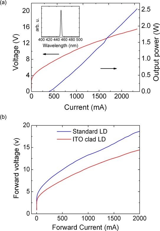
Figure 2: (a) Light output power, current and voltage (L-I-V) characteristics after facet coating for laser diode. Inset: lasing spectra. (b) Comparing I-V curves of laser diodes with and without ITO cladding.
The team estimates that optical power density at the front mirror with 2.52W operation was 94.43MW/cm2. The COMD power density for c-plane InGaN laser diodes have been reported in the range 40-70MW/cm2. GaAs-based devices have been reported with COMD of 30MW/cm2 under single-pulse excitation.
The researchers point out that the peak output power of their device was not limited by thermal roll-over or COMD, but rather by power-supply limitations to currents less than 2.34A.
In terms of current–voltage performance, the reduction in GaN cladding enabled by the use of ITO reduced the forward voltage somewhat, but the peak wall-plug efficiency was still low at 7.3%.
Indium tin oxide cladding InGaN Laser diodes MOCVD GaAs substrates
http://dx.doi.org/10.1063/1.4915324
The author Mike Cooke is a freelance technology journalist who has worked in the semiconductor and advanced technology sectors since 1997.


