


- News
8 April 2015
Indium arsenide quantum well laser diodes with 2.9μm wavelength
Shanghai Institute of Microsystem and Information Technology has developed a long-wavelength indium arsenide (InAs) quantum well (QW) laser diode (LD) grown on indium phosphide (InP) substrate [Y. Gu et al, Appl. Phys. Lett., vol106, p121102, 2015]. The researchers claim the longest wavelength achieved (2.9μm) as a record for antimony-free (Sb) structures.
Among the applications the researchers have in view are molecular spectroscopy gas analysis and medical inspection. These require wavelengths longer than 2.4μm and up into the mid-infrared (3-5μm).
Antimony-based semiconductor lasers can achieve 3μm continuous wave (CW) operation at room temperature, using gallium antimonide (GaSb) substrates. However, GaSb is more expensive than InP and presently is of lower quality. Further, GaSb-based devices suffer thermal management problems due to low thermal conductivity.
Gas-source molecular beam epitaxy (GS-MBE) was used to grow the laser structure (Figure 1) on sulfur-doped (001) n-InP. A template/cladding layer of 0.87μm metamorphic n-In0.8Al0.2As (485°C) was grown on 1.6μm compositionally graded InAlAs buffer (495°C-455°C) on top of In0.52Al0.48As, which is lattice-matched with the underlying InP substrate. The indium-content grading went from 52% to 84%, overshooting the 80% of the metamorphic template layer. The overshoot was designed to ensure full relaxation of the template layer. The n- and p-type doping for InAlAs layers were provided by silicon and beryllium, respectively.
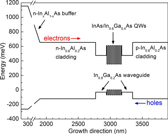
Figure 1: Energy-band structure of InP-based metamorphic type-I QW laser. Injection directions of electrons and holes are indicated.
The active region features a quantum well structure with eight 15nm InAs wells in 15nm In0.6Ga0.4As barriers, grown at 435°C. The QW material composition and thicknesses were designed to provide strain compensation with respect to the template. The use of eight wells compensated for the impact on radiative recombination from the relatively large density of threading dislocations (106-107/cm2) in the template layer.
In0.8Ga0.2As was chosen for the waveguide material, which has been found to have better performance than In0.8Al0.2As or In0.8AlyGa1-yAs alternatives. The upper p-InAlAs cladding was 1.8μm, followed by 300nm p-In0.8Ga0.2As for the contact. The waveguide, cladding and contact were grown at 465°C.
Ridge waveguide laser diodes were produced with 8μm-wide ridges. Isolation was provided by 300nm of silicon nitride. Finished devices were mounted epi-side up on copper heat-sinks. The measurements were made with the devices in a liquid nitrogen cryostat.
A laser diode with a 0.8mm-long cavity lased at around 2.80μm at 160K under 200ns 100kHz pulsed operation at 1.2x the threshold current. The wavelength red-shifted to 2.91μm at 230K, "by far the longest wavelength of InP-based type-I QW lasers," according to the research team.
Continuous-wave operation was limited to less than 180K due to self-heating effects. The 150K CW output power was 1.2mW/facet at a 400mA injection current. The CW lasing operation voltage was ~1V at 150K and ~1.2V at 180K.
The pulsed and CW current density thresholds at 120K were 812A/cm2 and 797A/cm2, respectively (Figure 1). The increase in threshold for pulsed operation had a characteristic temperature (T0) of around 60K between 120K and 200K. The corresponding figure for CW injection was 53K. Above 200K, T0 for pulsed operation decreased to 17K. This drop is attributed to increased carrier loss.
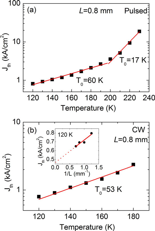
Figure 2: Temperature dependence of threshold current density of laser with 0.8mm cavity length under (a) pulsed and (b) CW operation. Inset of figure (b): CW threshold current density (Jth) as function of reciprocal cavity length (1/L) at 120K. Solid and dotted lines are fits to experimental data and extrapolation, respectively.
Extrapolating the CW threshold current at 120K to infinite cavity length gave a value of 465A/cm2. The 1.4mm cavity threshold was 650A/cm2.
The researchers say that they need to improve carrier confinement to increase operation temperatures. Electron and hole leakage could be reduced with blocking layers on the n- and p-sides of the device. The researchers describe their work as being at an early stage.
InAs quantum well laser diodes InAs MBE InP substrate
http://scitation.aip.org/content/aip/journal/apl/106/12/10.1063/1.4916270
The author Mike Cooke is a freelance technology journalist who has worked in the semiconductor and advanced technology sectors since 1997.


