


- News
29 April 2015
Red lasers from III-nitride nanowire forests on silicon
Researchers in USA and Saudi Arabia have been producing 610nm-wavelength red lasers with III-nitride nanowires (NWs) grown on silicon [Shafat Jahangir et al, Appl. Phys. Lett., vol106, p071108, 2015]. With a view to plastic fiber optical communication, the team from University of Michigan and King Abdullah University of Science and Technology (KAUST) studied the small-signal modulation characteristics.
Other potential applications include mobile projectors, head-up displays in automobiles, and photodynamic therapy. Production on silicon promises lower-cost production and mass manufacturing.
The array of vertical nanowires was produced on (001) n-type silicon using molecular beam epitaxy (MBE). The disk-in-nanowire structure was grown along the c-direction (Figure 1). The gain medium consisted of a 6-period structure with 2nm indium gallium nitride (In0.51Ga0.49N) disks in 12nm gallium nitride (GaN) barriers.
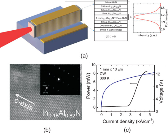
Figure 1: (a) Schematic of nanowire array laser heterostructure with calculated mode profile; (b) high-resolution transmission electron micrograph (HRTEM) of In0.18Al0.82N nanowire showing relatively defect-free crystal structure along growth direction. Inset: selective-area diffraction pattern from HRTEM study. (c) Light-current-voltage characteristics from 10μmx1mm laser at room temperature.
The GaN regions of the device were grown at 800°C. The InGaN disk region was deposited at 545°C. The lattice-matched indium aluminium nitride (In0.18Al0.82N) cladding layers were applied at 510°C. InAlN was chosen to improve optical confinement over AlGaN.
The average nanowire had 60nm diameter and 800nm height. The random array density was 2x10¹⁰/cm2 with 7nm average spacing.
Ridge waveguide laser were produced from the epitaxial nanowire arrays. Mesas were produced with plasma etching. Conformal parylene was applied to planarize the structures and passivate the nanowires. The GaN tips of the nanowires were left exposed for ohmic p-contacts with nickel/gold (5nm/5nm) followed with 250nm indium tin oxide (ITO). The n-contact was through aluminium deposited on the bare region of the n-silicon substrate.
The laser cavity was cleaved with perpendicular facets, which were flattened with focused ion-beam (FIB) etching and coated with titanium dioxide/silicon dioxide distributed Bragg reflectors (DBRs) of reflectivity ~0.35 and ~0.95.
A device with a 1mm cavity and 10μm-wide ridge had a 2.9A/cm2 threshold current density at room temperature under continuous-wave operation. The output-slope and wall-plug efficiencies were 2.5% (~0.1/A) and 0.2%, respectively.
The peak emission mode wavelength was around 610nm with a minimum linewidth of 9Å. The wavelength blue-shifted by 14.8nm when the current density increased between 1.4kA/cm2 and 3.6kA/cm2.
Temperature-dependent measurements of the threshold current gave a T0 characteristic temperature of 234K. The researchers comment: "The large value of T0 indicates good thermal stability in these devices. This value of T0 is comparable with those measured in red-emitting self-assembled InGaN/GaN quantum dot lasers."
Sub-threshold Hakki-Paoli optical gain measurements suggested the presence of InGaN quantum dots in the gain region. The researchers add: "The formation of self-organized islands in the InGaN disk region, which behave as quantum dots, has been confirmed by us by transmission electron microscopy (TEM) and the observation of single photon emission."
Modulation measurements were made on a 4μmx400μm device (Figure 2). The differential gain was 3.1x10⁻¹⁷cm2, according to the current-dependence of the resonance frequency, assuming radiative efficiency of 0.52 and confinement factor of 0.018. The differential gain "compares favorably with the differential gain of red-emitting self-organized quantum dot lasers," according to the researchers.
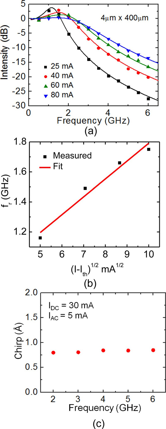
Figure 2: (a) Measured small-signal modulation response of a 400μmx4μm nanowire ridge waveguide laser for varying DC injection currents; (b) resonance frequency, fr, versus square root of injection current; (c) measured chirp as function of small-signal modulation frequency.
The chirp under small-signal modulation was around 0.8Å up to 6GHz. The researchers comment: "The low value of chirp is very encouraging in the context of optical communication in plastic fibers. Chirp is usually small in lasers with quantum-confined gain media. Furthermore, in GaN and related materials, the change in refractive index with carrier injection is small."
The f-3dB,max maximum modulation bandwidth was 3.1GHz.
http://dx.doi.org/10.1063/1.4913317
The author Mike Cooke is a freelance technology journalist who has worked in the semiconductor and advanced technology sectors since 1997.


