


- News
24 September 2014
Single-crystal gallium arsenide on metal foil
Researchers in USA have produced single-crystal gallium arsenide (GaAs) films on metal foil with a view to low-cost roll-to-roll production of optoelectronic devices such as high-efficiency solar cells [P. Dutta et al, Appl. Phys. Lett., vol105, p092104, 2014]. Doped films were produced with high carrier mobility.
The research was carried out at University of Houston, South Dakota School of Mines and Technology, and NASA Johnson Space Center. Although high-efficiency solar cells are based on direct-bandgap GaAs, such devices tend to be expensive to produce. It is estimated that more than half the production cost of GaAs solar cells comes from the expensive GaAs or germanium (Ge) substrates used.
High cost restricts GaAs solar cells to specialist applications such as space satellites, where payload weight is at a premium. For earth-bound application, production cost is generally the primary consideration and therefore the much less efficient silicon technology is the standard.
The US researchers comment on their work: “High-quality single-crystalline GaAs thin film on inexpensive metal foil can be a promising step towards high-efficiency and cost-effective thin-film III-V solar cells and can eventually pave the path for scalable large-area processing of III-V solar cells for terrestrial applications.”
Templates for the GaAs crystal film consisted of germanium grown on Hastelloy metal foil using sputtering and ion-beam-assisted deposition (Figure 1). For the GaAs deposition, the researchers used a custom-made vertical metal-organic chemical vapor deposition (MOCVD) reactor. The system employed radio-frequency induction heating. The single-crystalline-like Ge templates were loaded into the system on graphite susceptors.
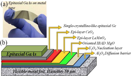
Figure. 1: (a) Photograph of epitaxial GaAs thin film on flexible metal foil. (b) Schematic of multi-layer template architecture used to grow epitaxial GaAs thin films on metal foil.
The GaAs MOCVD precursors were trimethyl gallium and arsine (ArH3) in hydrogen carrier. Selenium (n-type) and zinc (p-type) doping was provided by diethyl-diselenide and dimethyl-zinc, respectively.
Before GaAs deposition, the Ge surface was pre-annealed in arsine at 650°C for 10 minutes to remove native oxide. During GaAs deposition, the substrate was rotated 400 times per minute in order to achieve a uniform film.
The optimum growth temperature was found to be 575°C. The chamber pressure was 20Torr. Doping concentration was controlled by varying the hydrogen dilution.
The researchers report: “The GaAs films were mechanically robust, exhibited good adhesion and no signs of cracking during bending tests, suggesting minimal effect of thermal mismatch and strain between the epilayers.” Further, electron diffraction analysis suggested that the film had a zincblende single-crystal structure.
The defect density of a p-GaAs film was estimated to be 3x10⁷/cm2. Similar values in the range 4-9x10⁷/cm2 were found for undoped- and n-GaAs. These values are about an order of magnitude higher than for GaAs grown on Ge wafer substrates. The researchers attribute the increase to the rougher template surface and higher defect density level in the ‘single-crystal-like’ Ge layer on metal foil.
Strong photoluminescence (PL) was seen in all the samples, with the undoped film giving a much stronger peak (Figure 2). The lower peaks in the doped samples were attributed to non-radiative recombination due to the presence of impurities.
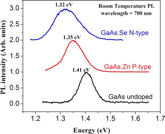
Figure 2: Room-temperature photoluminescence spectra of undoped, Zn- and Se-doped GaAs thin films on flexible metal foils.
In addition, the shape and position of PL peak changed between the undoped and doped GaAs films. The undoped GaAs peak was at 1.41eV, corresponding to bandgap transitions. The Zn-doped p-GaAs film had a peak at 1.35eV; the Se-doped n-GaAs layer at 1.32eV. The red-shift effect of doping was attributed to bandgap narrowing and/or residual strain from dopant incorporation.
The widths of the peaks in the doped films (0.125eV for n-GaAs, 0.085eV for p-GaAs) were also broader than for the undoped GaAs (0.061eV). Broader lines suggest higher densities of defects.
Hall measurements of mobility and carrier concentration were carried out on films grown on 200nm GaAs buffer layers to avoid the underlying Ge material from affecting the results. The undoped intrinsic GaAs films showed high resistivity of 106Ω-cm. The Zn-doped GaAs had a high 1019-1021/cm3 carrier concentration and 12-66cm2/V-s hole mobility. The Se-doped GaAs carrier concentration was 1017-1018/cm3 with electron mobility as high as 300cm2/V-s.
The high conductivity of (1-5)x104/Ω-cm of heavily Zn-doped GaAs films could find application as the base layer of flexible hetero-bipolar transistors (HBTs), tunnel diodes, back surface field, and emitter layer of solar cells and power transistors, according to the researchers.
The Se-doped GaAs showed a lower conductivity of 101-102/Ω-cm. The researchers comment: “Lightly doped n-type GaAs films with high carrier mobility can be utilized as base layers of solar cells. This is by far the highest reported electron mobility of crystalline GaAs film grown on flexible metal substrates by direct MOCVD.”
http://dx.doi.org/10.1063/1.4895388
The author Mike Cooke is a freelance technology journalist who has worked in the semiconductor and advanced technology sectors since 1997.


