


- News
22 September 2014
SDK boosts 6” SiC epi production capacity for power devices from 400 to 1100 wafers per month
Tokyo-based Showa Denko K.K. (SDK) has increased its capacity for producing 6-inch (150mm)-diameter silicon carbide (SiC) epitaxial wafers for use in power devices from 400 to 1100 wafers per month. SDK has hence increased its total SiC epiwafer production capacity in terms of 4-inch (100mm) wafer equivalents by about 60% from 1500 to 2500 wafers per month. Also, in October, SDK will start shipping a new grade of SiC epiwafer with fewer defects and higher uniformity.
Compared with mainstream silicon-based semiconductors, SiC power devices using SiC epiwafers can operate under relatively high-temperature, high-voltage and heavy-current conditions while substantially reducing energy loss, notes SDK. SiC power devices are hence regarded as next-generation power devices that enable the production of smaller, lighter and more efficient power control modules. Inverters based on SiC power devices are already used in applications such as power sources for servers in data centers, decentralized power generation systems utilizing new energy sources, and subway railcars. Moreover, some car makers and their suppliers have recently announced that they will use inverters based on SiC power devices in electric vehicles and hybrid electric vehicles (EVs/HEVs). Demand for SiC power devices is hence expected to rise.
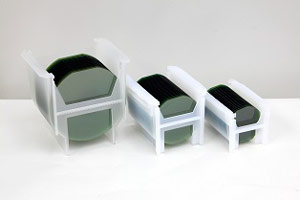 Picture: SiC epiwafers with (from left to right) diameters of 6, 4 and 3-inches.
SDK produces and sells 3” (76.2mm), 4” and 6” SiC epiwafers. To increase the supply of 6” wafers, which can help to increase power device manufacturing productivity, the firm has added chemical vapor deposition (CVD) equipment that can be applied to the production of all sizes of SiC epiwafers in its range. The new equipment improves epiwafer productivity by about 30%, further reducing power-device production costs.
SiC-based power control modules for use in automobiles, power generation facilities, power transmission facilities and high-speed trains are now required to have heavier withstanding currents, while market demand for the SiC power control modules is expected to grow in the near future. To meet these requirements, the enlargement of SiC chip size is necessary.
To prevent a deterioration of yield rates in producing large-sized SiC chips from epiwafers, in October SDK will begin selling a new grade of SiC epiwafer with fewer surface defects (0.25 defects/cm2 versus 0.5 defects/cm2 for current-grade wafers). The new-grade products should enable users to expect an improvement in yield rate of more than 10% in the production of large SiC chips for the above applications (as estimated for chips of 7-10mm2).
Showa Denko launching 6" SiC epiwafers for inverter power devices


