


- News
9 October 2014
Bendy blue LEDs on polymer without thermal budget restrictions
South Korea’s Seoul National University has developed flexible micro-rod light-emitting diodes (LEDs) using gallium nitride (GaN) grown on graphene [Kunook Chung et al, APL Mater., vol2, p092512, 2014]. The LED layers consisted of indium gallium nitride (InGaN) multiple quantum wells (MQWs).
Although inorganic compound semiconductor materials have been grown directly on flexible polymer substrates, the thermal budget is very tight. III-nitride semiconductors generally need high temperature for high-quality crystal growth. Seoul National University has used growth on graphene to enable easy release from an inorganic substrate and transfer to polymer as an alternative route to flexible devices.
The graphene was prepared on copper foil by chemical vapor deposition (CVD) and then transferred to silicon dioxide on silicon substrate. The GaN microrods were grown using metal-organic CVD (MOCVD) with trimethyl-gallium (TMGa), ditertiarybutyl-silane (DTBSi) and ammonia (NH3) precursors in nitrogen carrier. Two-step GaN growth at 750-850°C (3mins) and then 950-1050°C (30mins) was followed by annealing at 1100°C (10mins).
The hexagonal micro-rods were grown on a 2μm GaN buffer. The density of rods was 107/cm2. With the 30 minute growth time, the rods were 1μm in diameter and 7.5μm high. The buffer improved vertical alignment of the rods, allowing the fabrication of coaxial quantum wells.
The micro-rods exhibited near-band-edge photoluminescence at 3.4eV photon energy, and at higher pump powers they exhibited stimulated emission. There was also some weak deep-level emission around 2.2eV. Detailed micro-photoluminescence of a single rod showed no shift in the peak position in spectra from the top, middle and base regions of the rod, suggesting negligible strain fields.
An 8-period quantum well structure of In0.07Ga0.93N in GaN barriers was MOCVD coated coaxially onto the top and sidewalls of the n-type GaN micro-rods. The LED device structure was completed with a coaxial p-GaN layer. The well thickness was estimated at 8nm on the sidewalls and 4nm on the top of the rods. The emission wavelength from cathodoluminescence (electron beam excited) on the wells was 439nm from the top region and 414nm from the sidewalls, the difference arising from the varying well thickness.
LEDs were fabricated with metal contact deposition and transferred to polyimide (Figure 1). The rods were insulated from each other by a polyimide fill. Oxygen plasma etch exposed the tips of the rods. The metal contact to the p-GaN consisted of nickel/gold. The n-type titanium/gold contact was made to the base of the GaN buffer, after separation of the epitaxial material from the growth substrate by a wet buffered oxide etch (BOE). An addition thick silver layer was used to give reliable current injection.
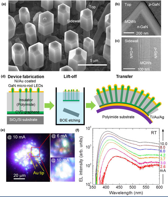
Figure 1: GaN micro-rod LEDs fabricated on graphene. (a) Field-emission scanning electron microscope image of coaxial GaN micro-rod LEDs on graphene. Scanning transmission electron microscope images of (b) top and (c) sidewall of MQW layers. (d) Schematic of fabrication process for vertical structure micro-rod LEDs. (e) Magnified optical images of light emission from LED. (f) Power-dependent electroluminescence spectra at room temperature.
The LEDs emitted strong blue light with orange and green from some rods at lower injection (6mA). The longer-wavelength emissions turned blue as the current injection increased beyond 10mA. The researchers attribute the orange/green emission to yellow emission in the p-GaN layer. The team believes the yellow emission source could be reduced by optimizing the material growth process.
The devices were also subjected to bending and the electroluminescence suffered no degradation from bending with a 6mm curvature radius. However, bending with a 4mm radius resulted in markedly decreased electroluminescence, suggesting damage from the bending.
LEDs GaN Graphene GaN on graphene InGaN InGaN MQWs CVD MOCVD
http://dx.doi.org/10.1063/1.4894780
The author Mike Cooke is a freelance technology journalist who has worked in the semiconductor and advanced technology sectors since 1997.


