


- News
12 November 2014
Thicker InGaN wells enabled by semi-polar (30-3-1) substrate
University of California Santa Barbara (UCSB) and Mitsubishi Chemical Corp have reported indium gallium nitride (InGaN) light-emitting diodes (LEDs) with thicker active regions enabled by growing the crystal on the semi-polar (30-3-1) plane [Daniel L. Becerra et al, Appl. Phys. Lett., vol105, p171106, 2014].
Normal InGaN devices grown on the polar c-plane are restricted to well thicknesses of a few nanometers. These thicknesses are required to avoid the electron-hole separation arising from the high electric fields that result from the strong polarization of the bonds in III-nitride materials – giving rise to the quantum-confined Stark effect (QCSE).
The need to confine the carriers in thin wells results in high carrier densities that encourage alternative non-radiative (‘Auger-like’) recombination, reducing the conversion efficiency of electrical power into light (‘efficiency droop’).
The use of (30-3-1) material allowed the researchers to create wells between 10nm and 100nm thick, while maintaining electron-hole wavefunction overlap. The device material (Figure 1) was grown on semi-polar (30-3-1) free-standing GaN substrates by metal-organic chemical vapor deposition (MOCVD). The substrates came from Mitsubishi Chemical.
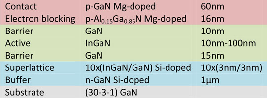
Figure 1: Heteroepitaxial structure.
Calculations of the band structure for a 10nm-thick In0.12Ga0.88N active region suggested that the single well structure would have a much better electron-hole overlap compared with the same structure grown on c-plane material. Theoretical considerations also suggested that thicker layers of InGaN could be grown on (30-3-1) material before misfit dislocation formation at heterointerfaces would become a problem.
In fact, the researchers found an increased critical thickness for misfit dislocation formation of 30nm for (30-3-1) In0.1Ga0.9N, compared with 20nm for semi-polar (20-2-1) InGaN – a crystal orientation that UCSB has experimented with extensively. Further, the impact on electroluminescence of increasing the active region thickness beyond the critical value was much less severe when comparing (30-3-1) with (20-2-1) devices.
LEDs were formed with 0.1mm2 rectangular active region mesas. The p-contact was covered with indium tin oxide (ITO) transparent current-spreading material. The n-contact metals were titanium/aluminium/nickel/gold. Contact pads consisted of chromium/nickel/gold. The back-side of the device was roughened, presumably to improve light extraction. The LEDs were mounted on silver headers and encapsulated in silicone.
Although 10nm single wells demonstrated the peak external quantum efficiency (EQE) under pulsed current operation, devices with 20-40nm demonstrated higher EQEs at higher injection currents (Figure 2). Pulsed current operation is used to avoid performance degradation from self-heating effects.
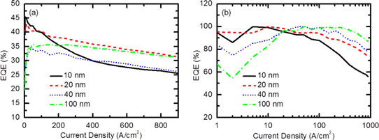
Figure 2: (a) Absolute EQE versus current density and (b) normalized EQE versus current density on a logarithmic scale for LED devices with active region thickness 10-100nm (pulsed condition, 1% duty cycle).
The thermal droop effect was also measured by subjecting the devices to different temperatures (Figure 3). The ratio of EQEs at 100°C and 20°C (‘hot/cold factor’) was around 0.9 for well thicknesses in the range 10-40nm. Thicker wells of 100nm had more thermal droop with a 0.8 hot/cold factor.
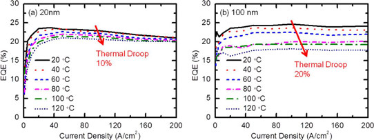
Figure 3: EQE versus current density measured at different temperatures for devices with (a) 20nm- and (b) 100nm-thick active regions.
A 15nm-well device was assembled into an optimized vertical transparent package, achieving an EQE of more than 50%. At 1kA/cm2 current density, the device had an EQE of 33% and light output power of 1008.7mW. The wavelength of the emission was around 412nm with a narrow linewidth of ~16nm, full-width half maximum. Up to 1kA/cm2, the wavelength shift was small, of the order of nanometers.
InGaN LEDs InGaN LEDs Efficiency droop GaN substrates MOCVD
http://dx.doi.org/10.1063/1.4900793
The author Mike Cooke is a freelance technology journalist who has worked in the semiconductor and advanced technology sectors since 1997.


