


- News
6 November 2014
GaAs/InP wafer bonding with low electrical resistance
Researchers based in Japan and China have developed a room-temperature wafer bonding process for gallium arsenide (GaAs) and indium phosphide (InP) with ‘extremely low resistance’ [Shiro Uchida et al, Appl. Phys. Express, vol7, p112301, 2014]. The team from Sony Corp and Suzhou Institute of Nano-tech and Nano-bionics see their process as being “a promising technique for fabricating multi-junction solar cells with more than four junctions in order to obtain high conversion efficiencies.”
Up to now, wafer bonding techniques have added unacceptable levels of electrical resistance to multi-junction solar cell structures, limiting the options for creating photovoltaic sub-cells. In their new research, the Sony/Suzhou team found that bonding n-type GaAs and n-type InP resulted in unwanted diode-like current-voltage performance, but paradoxically that bonding p+-GaAs to n-InP gave an ohmic contact. In addition, the researchers claim the lowest resistance yet achieved for GaAs/InP wafer bonding.
Although some groups have used higher-temperature bonding (400-700°C) to lower the resistance of GaAs/InP bonded wafers, the ohmic values have still been higher than desired. Lower-temperature processes also avoid structural problems such as wafer bending, defects, voids, and cracks.
In solar cell applications, the heavily doped p+-GaAs layer would need to be as thin as possible to reduce optical losses due to free carrier absorption. However, in these first experiments the researchers used 450μm p+-GaAs substrates.
The researchers bonded zinc-doped p+-GaAs and 600μm-thick sulfur-doped n-InP wafers in Mitsubishi Heavy Industries’ MWB-06-R room-temperature wafer bonding machine. The equipment includes an argon ion gun to activate the wafer surfaces and to form dangling bonds. The wafers were prepared for bonding with an alkali cleaning solution. The bonding force was 5000N.
Ohmic contacts of titanium/platinum/gold were applied to the remaining surfaces of the bonded wafers. The contact metals were alloyed at the relatively low temperature of 260°C. The material was diced into 3mmx3mm chips for testing.
The resistance across the bond was estimated to be 1x10⁻³Ω (8.9x10⁻⁵Ω-cm2), after correcting for the resistance of the materials and the metal contacts. The resistance of the whole structure was 6.7x10⁻³Ω with good ohmic current-voltage linearity (Figure 1).
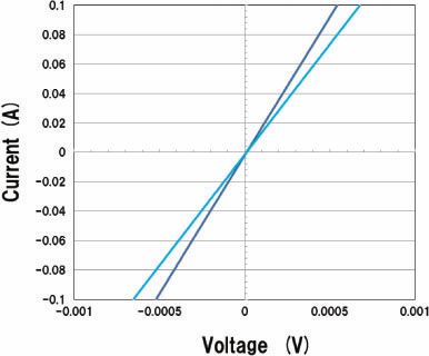
Figure 1: Characteristics for 3mmx3mm p+-GaAs/n-InP bonded samples fabricated under (a) conventional and (b) optimized conditions.
The researchers achieved a lower resistance through the bond of 2.8x10⁻⁴Ω (2.5x10⁻⁵Ω-cm2) by optimizing bonding time, temperature, applied voltage, and applied pressure, along with increasing the alloying temperature of the ohmic contacts to 340°C. “To the best of our knowledge, this is the lowest interface resistance ever reported for a direct GaAs/InP bond,” the researchers comment.
Since solar cells should be designed to operate at high current density, the researchers tested 0.5mmx0.5mm chips at high current (Figure 2). The chips operated at up to 200A/cm2 without breakdown, a much greater density than that needed for concentrated sunlight photovoltaics (>5A/cm2).
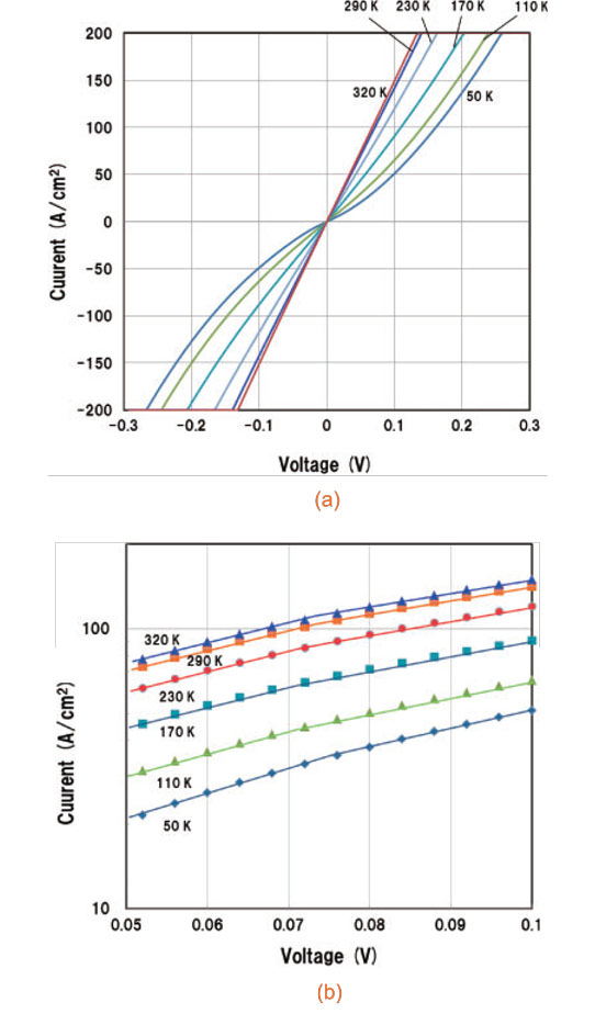
Figure 2: Characteristics for 0.5mmx0.5mm p+-GaAs/n-InP bonded samples between 50K and 320K for (a) currents between -200A/cm2 and 200A/cm2 and (b) bias voltages between 0.5 and 1.0V.
The researchers believe that the ohmic current-voltage characteristics of the p+-GaAs/n-InP bond was the result of a complex combination of tunnel and trap-assisted currents. Analysis of the bond region found an amorphous interlayer region where one would expect a high density of interfacial defect states.
The researchers also produced bonds with thin interlayers of titanium between the p+-GaAs and n-InP wafers. The resistance across the bond was ohmic (1.5x10⁻³Ω for p+-GaAs/2.0nm Ti/2.0nmTi/n-InP), but higher than for chips without titanium interlayers.
GaAs/InP wafer bonding Multi-junction solar cell GaAs InP
http://dx.doi.org/10.7567/APEX.7.112301
The author Mike Cooke is a freelance technology journalist who has worked in the semiconductor and advanced technology sectors since 1997.


