


- News
26 November 2014
Millimeter-wave performance of gallium nitride transistors on silicon
Researchers in Switzerland have reported the first large-signal 94GHz operation of aluminium indium nitride/gallium nitride (AlInN/GaN) high-electron-mobility transistors (HEMTs) on high-resistance (HR) silicon [Diego Marti et al, IEEE Electron Device Letters, published online 4 November 2014]. The team was based at ETH-Zürich and École Polytechnique Fédérale de Lausanne.
Better performance has been achieved in AlInN/GaN HEMTs on the extremely expensive silicon carbide (SiC) substrates due to the better lattice match between SiC and GaN. However, the team believes that GaN transistors built on silicon could lead to low-cost millimeter-wave applications.
The 94GHz frequency falls in the W-band (75-110GHz), which is used for satellite communications, millimeter-wave radar research, military radar targeting and tracking, and some non-military applications. There is an atmospheric window at 94GHz. One 94GHz application is passive cameras for concealed weapon detection. Cruise control radar for automobiles uses 77GHz.
Up to now, GaN HEMTs on silicon have been restricted to K/Ka-band (less than 40GHz) performance.
The epitaxial material (Figure 1) was grown on 50mm float-zone-refined high-resistance (10kΩ-cm) silicon (111) substrates. The two-dimensional electron gas (2DEG) channel near the aluminium indium nitride (AlInN)/gallium nitride barrier/buffer interface had a Hall mobility of 1190cm2/V-s. Van der Pauw measurements gave a sheet resistance of 328Ω/square, corresponding to a sheet carrier density of 1.6x10¹³/cm2.
Figure 1: Epitaxial material structure.
| Cap | GaN | 2nm |
| Barrier | Al0.83In0.17N | 3.5nm |
| Spacer | AlN | 1nm |
| Buffer/channel | GaN | 1μm |
| Transition | Graded AlGaN | 1μm |
| Nucleation | AlN | |
| Substrate | HR-Si (111) |
Transistors were fabricated through plasma etch mesa isolation, source-drain contact re-growth of n+-GaN, deposition of titanium/platinum/gold metal ohmic contacts, and nickel/platinum/gold T-gate formation.
The re-growth used a silicon dioxide mask and ammonia molecular beam epitaxy (MBE). The gate footprint was 50nm long and 2x50μm wide. The gate stem and head were 200nm high and 500nm wide, respectively.
The source-drain and source-gate separations were 2μm and 0.5μm, respectively. The relatively large source-drain separation and short gate length were chosen to reduce current-collapse effects of pulsed/high-frequency operation. Although field plates are often used to avoid current collapse, the ETH/EPFL device did not have any.
A 75nm layer of silicon nitride was deposited for passivation. Contact pads consisted of titanium/gold.
A maximum DC drain current of 1.6A/mm was achieved at +2V gate potential. The peak transconductance was 650mS/mm at 5V drain bias and -1.5V gate potential. The on-resistance was 1.19Ω-mm. Gate leakage with a -5V gate potential was 250μA/mm.
The researchers comment: “Because the gate length is only 50nm and because of the lack of a channel back-barrier, the channel pinch-off is incomplete at higher VDS, though it remains adequate for the class A operating voltages considered here.”
Pulsed measurements gave a higher maximum drain current of 2A/mm – the lower value for the DC measurement is attributed to self-heating effects.
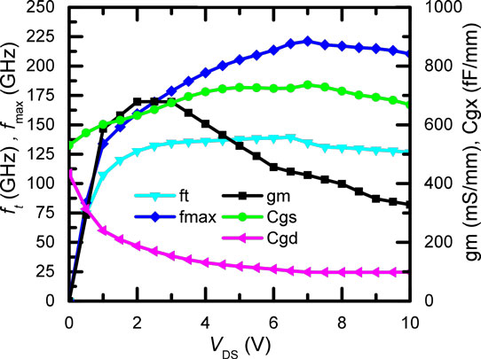
Figure 2: Drain voltage (VDS) dependence of small-signal performance at gate potential (VGS) -1.25V.
Small-signal frequency analysis of the performance (Figure 2) gave a peak cut-off frequency (fT) of 118GHz and maximum oscillation (fmax) of 210GHz. De-embedding the parasitic effect of the pads upgrades these values to 141GHz and 232GHz, respectively.
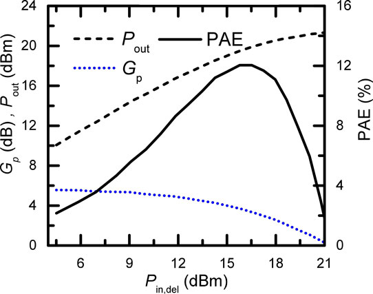
Figure 3: Power sweep of HEMT at 94GHz.
The 94GHz large-signal performance (Figure 3) showed a maximum power gain of 6dB. The peak power-added efficiency (PAE) of 12% was achieved with 1W/mm output power and 4dB associated power gain. The saturated output power was 1.35W/mm. The bias conditions were 1.2V on the gate and 9V on the drain.
A 3-stage power amplifier consisting of GaN transistors built on silicon carbide has achieved a PAE of 19% with 2.138W output power at 93.5GHz.
“The chosen bias point results from a trade-off between maximizing the drain-source voltage and keeping the current collapse reasonably small,” the researchers write.
The researchers believe that further refinement of the epitaxial structure and passivation aimed at reducing current collapse and short-channel effects could further improve performance.
http://ieeexplore.ieee.org/xpl/articleDetails.jsp?arnumber=6945795
The author Mike Cooke is a freelance technology journalist who has worked in the semiconductor and advanced technology sectors since 1997.


