


- News
21 May 2014
Indium gallium phosphide as top-cell for 4+ junction solar energy conversion
Yale University in the USA has developed indium gallium phosphide (InGaP) solar cells on gallium phosphide substrates [S. Tomasulo et al, Appl. Phys. Lett., vol104, p173903, 2014]. The aim of the researchers’ work was to create a top-cell option for multi-junction cells with four or more junctions in monolithic or spectrum-splitting architectures. It is hoped that such arrangements will be able to achieve conversion efficiencies up to almost 60%.
Such top cells need an energy bandgap of around 2.0-2.4eV. Gallium phosphide has such a bandgap, but unfortunately the 2.26eV gap is indirect, leading to inefficient conversion of photons into electrical energy. The InGaP alloy system has a transition from indirect to direct bandgap when the indium fraction exceeds 30%. However, the increase in indium content also leads to a reduction in the bandgap.
In fact, there are two valleys in the GaP bandstructure - a direct ‘gamma’ (Γ) valley giving a gap of 2.78eV and the indirect ‘chi’ (Χ) valley. In InGaP, the bandgap between the Γ valley and the valence band decreases at 19meV/% of indium. The Χ gap reduces more slowly at 1.7meV/%.
The Yale group explored how moving the composition towards the crossover point increases conversion efficiency. In fact, the conversion efficiency improves even in the indirect region as the Γ valley comes into range of the Χ valley. In germanium solar cells such ‘pseudo-direct’ proximity between the smallest indirect gap (0.66eV) and direct gap (0.8eV) leads to improved conversion.
Previous work with InGaP has tended to grow the material on gallium arsenide (GaAs) substrate. Unfortunately, the InGaP is then placed under tensile strain, which “leads to faceted trenches and cracks, and extremely thick graded buffers are required to minimize these efficiency-diminishing defects”. The Yale group chose GaP substrates so that the InGaP was under compressive strain to avoid these problems.
The epitaxial structures (Figure 1) were grown on p-GaP substrates in a Veeco Mod Gen II solid-source molecular beam epitaxy (MBE) chamber. The use of a gallium arsenide phosphide (GaAsP) graded buffer reduced threading dislocations that arise from the lattice mismatch between the substrate and overlying epitaxial structure. The compressive grading was achieved using between 10 and 16 steps of 360nm thickness and increased arsenic molar fraction of four percentage points per step. The aim was a grading rate of strain over buffer thickness of 0.4%/μm. The indium aluminium phosphide (InAlP) window layer was lattice-matched to the InGaP active emitter/base material.
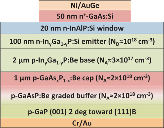
Figure 1. Schematic of InGaP solar cells.
The epitaxial samples were formed into 1mm x 1mm solar cells. The devices were patterned with photolithography and wet etched down to the n-InAlP window layer through the top n+-GaAs used to achieve good ohmic contact with the metal n-type electrodes. No anti-reflective coatings were used in any device. A reference GaP device with Al0.25Ga0.75P window was also produced.
The current and voltage characteristics were measured under AM1.5G solar simulation conditions (Table 1). Also, the theading dislocation density (TDD) was estimated using electron-beam-induced current (EBIC) measurements. The TDD increased by 3x with indium fractions between 18% and 30% - a factor that Yale plans to address in future work.
Table 1: Summary results: bandgap energy (Eg), threading dislocation density (TDD), open-circuit voltage (Voc), bandgap-voltage offset (Woc = Eg/q - Voc), short-circuit current density (Jsc), ratio of Jsc to theoretical maximum for infinite base and unity collection probability (Jsc,ratio), fill factor (FF), and conversion efficiency (η).
| Indium fraction | Eg (eV) | TDD (/cm2) | Voc (V) | Woc (V) | Jsc (mA/cm2) | Jsc,ratio | FF | η |
| 0% | 2.26a | . . . | 1.46 | 0.80 | 1.64 | 17% | 0.64 | 1.53% |
| 18% | 2.23a | 2.28x10⁶ | 1.46 | 0.77 | 2.29 | 23% | 0.74 | 2.47% |
| 24% | 2.21 | 4.02x10⁶ | 1.43 | 0.78 | 2.75 | 26% | 0.73 | 2.87% |
| 30% | 2.12 | 7.60x10⁶ | 1.42 | 0.70 | 3.65 | 30% | 0.75 | 3.89% |
a Indirect gap.
Although the devices are in the ambiguous direct-indirect bandgap region, their external quantum efficiency (EQE) behavior is similar to that of a direct-gap In0.49Ga0.51P device with a sharp turn-on at the band edge. The bandgap-voltage offsets (Woc) were higher than for InGaP on GaAs cells. The researchers comment: “We speculate that the wide-Eg solar cells presented here, as well as GaP devices, possess increased point defect densities, resulting in elevated Woc. It is possible that as y decreases, the growth conditions that were chosen for y = 0.49 are no longer appropriate, suggesting that growth condition optimization should be performed for each composition.”
The main improvement of the InGaP structure is an increase in short-circuit current density (Jsc), leading to a 2x improvement in conversion efficiency (η) over a GaP cell.
InGaP solar cells GaP substrates Multi-junction solar cells
http://dx.doi.org/10.1063/1.4874615
The author Mike Cooke is a freelance technology journalist who has worked in the semiconductor and advanced technology sectors since 1997.


