


- News
28 May 2014
Simplifying zinc oxide/gallium nitride nano-rod LED fabrication
Researchers in Taiwan have produced zinc oxide/gallium nitride (ZnO/GaN) nano-rod light-emitting diodes [Ya-Ju Lee et al, APL Mater. vol2, p056101, 2014]. The researchers avoided complicated polymer processing by using a shadowing effect to selectively deposit ZnO on GaN nanorods.
Often nano-rod-based devices are fabricated by filling the space between the rods with polymer and etching down to expose the tips to make an electrical contact. The team from National Taiwan Normal University, National Chiao-Tung University, National Taiwan Ocean University, and National Cheng Kung University comment that their method “allows us to overcome the constrictions of using a polymer, rendering our technique low cost and reliable for mass-production of nanoscale optoelectronic devices.”
The metal-organic chemical vapor deposition (MOCVD) GaN layers consisted of 2μm undoped material on sapphire substrate, followed by 400nm of p-type GaN. The hole concentration and mobility of the p-GaN were 5.5x10¹⁷/cm3 and 6.2cm2/V-s, respectively.
Nano-rod random arrays were fabricated in the p-GaN by depositing self-assembled nickel clusters on the surface and etching with inductively coupled plasma. The p-contact region was protected with a photolithography-defined mask. The nano-rods were 300nm long and 100-140nm in diameter. The number density of nano-rods was estimated to be 2.2x10⁹/cm2, representing a 17.3% volume filling.
The ZnO was deposited using oblique-angle radio-frequency (RF) magnetron sputtering at room temperature. The nano-rods were tilted at 60° with respect to the ZnO vapor flow. The p-GaN nano-rod array provides the shadowing effect so that the ZnO is deposited selectively on the nano-rod tips. The sample was annealed after ZnO deposition to ameliorate the effects of defects and surface states. The ZnO had an n-type characteristic with an electron density of 7.4x10¹⁸/cm3 and mobility of 3.9cm2/V-s.
Indium tin oxide (ITO) was then deposited by RF magnetron sputtering at a -60° tilt to provide a continuous transparent conductive contact and current-spreading layer connecting the individual n-ZnO/p-GaN nano-rod junctions together. Individual devices were fabricated with a chip size of 300μmx400μm (Figure 1).
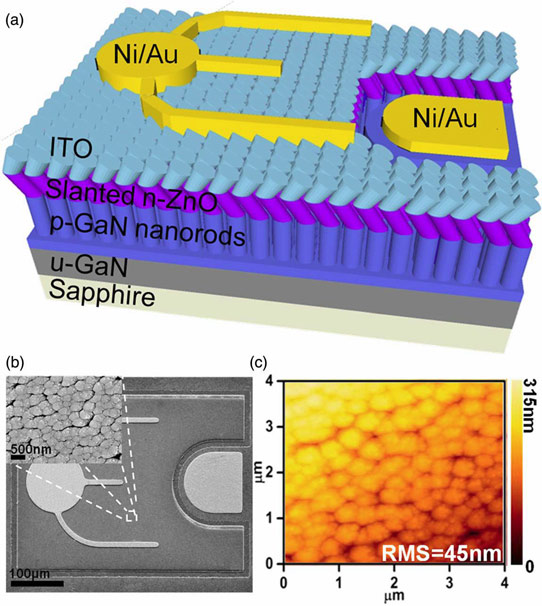
Figure 1: (a) Design of LED composed of slanted n-ZnO film on p-GaN nanorod arrays. An additional slanted ITO film interconnects slanted n-ZnO/p-GaN nanorod arrays for electrical injection. (b) Top-view SEM image of fabricated LED. Inset: enlarged top-view SEM image of surface of slanted ITO film. (c) Atomic force microscope (AFM) image of slanted ITO film.
The device showed good diode behavior with a turn-on voltage of 4.7V. The device emits a bluish-white light visible to the naked eye. The wall-plug efficiency peaks at around 4mA. The fall-off could be due to overheating of the device. The spectrum (Figure 2) was found to consist of two main peaks centered at 390nm (violet) and 485nm (green). The researchers associate the shorter wavelength to near-band-edge emission in the ZnO. They add: “The 485nm emission is probably related to the radiative interfacial recombination of the electrons from slanted n-ZnO and holes from p-GaN nanorod arrays, or to the energy transition from a shallow donor level to the VZn [zinc vacancy] level.”
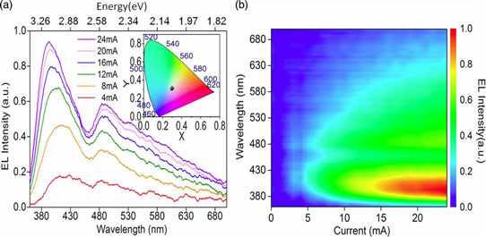
Figure 2: (a) EL spectra of slanted n-ZnO/p-GaN nanorod arrays LED for various injection currents. Inset: calculated CIE chromaticity ordinates of EL spectra. (b) Same EL spectra converted and re-plotted as 3D contour image.
The CIE color coordinates were (0.3, 0.3). The researchers suggest that such structures could be developed as white-light sources.
Zinc oxide gallium nitride nano-rod LED GaN ZnO MOCVD
http://dx.doi.org/10.1063/1.4874455
The author Mike Cooke is a freelance technology journalist who has worked in the semiconductor and advanced technology sectors since 1997.


