


- News
21 March 2014
Monolithic integration of nitride semiconductor HEMTs and LEDs
Hong Kong University of Science and Technology (HKUST) is developing techniques to monolithically integrate high-electron-mobility transistors (HEMTs) and light-emitting diodes (LEDs) based on aluminium indium gallium nitride (AlInGaN) semiconductor materials [Zhaojun Liu et al, Appl. Phys. Lett., vol104, p091103, 2014].
The researchers believe that the HEMT-LED integration could find applications in smart lighting, LED micro-displays and visible light communication. Nitride semiconductor HEMTs have the potential to provide superior power management over silicon-based conventional AC-DC conversion through pulse-width modulation or analog current control. Nitride semiconductor transistors enable higher breakdown voltages, higher operating frequencies and wider operating temperatures.
The researchers comment: “Sharing the same GaN-based material platform, monolithic integration of LEDs and HEMTs can potentially reduce the form factor and manufacturing cost of an LED lighting system and greatly improve the system stability and reliability.”
However, integration brings challenges in terms of different optimal growth temperatures for AlGaN/GaN HEMTs and InGaN/GaN LEDs. Further problems arise in device fabrication with potential damage from plasma etch processing.
The HKUST HEMT structures were grown on commercial 2-inch LED wafers by metal-organic chemical vapor deposition (MOCVD). The GaN buffer was 170nm, the u-AlGaN back-barrier was 55nm, the u-GaN channel was 200nm, the AlN spacer was 1nm, and the AlGaN top barrier was 20nm. Two methods for integrating HEMTs were compared: growth of the epitaxial layers followed by selective epitaxial removal (SER), leaving HEMT material adjacent to the LED regions; or, deposition and patterning of a silicon dioxide mask, followed by selective epitaxial growth (SEG) of the HEMT layers.
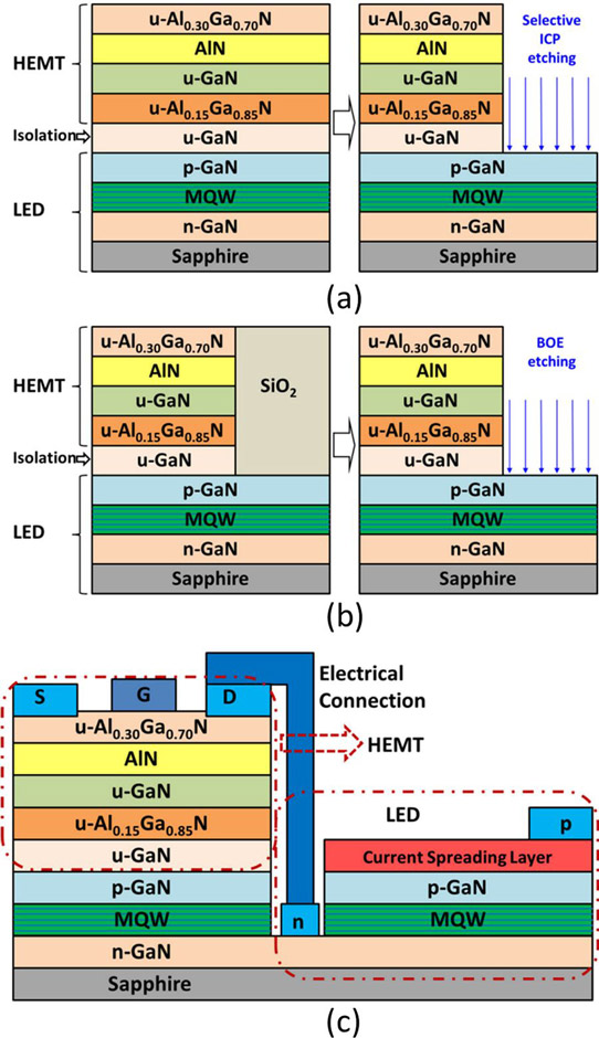
Figure 1: Schematic cross-section of (a) selective epi removal (SER), (b) selective epi growth (SEG), and (c) final structure of HEMT-LED.
The SER method used inductively coupled plasma to open a window for the LED. For the SEG method, the silicon dioxide mask was removed with a wet buffered oxide etch. Comparison HEMTs were also produced separately on sapphire substrates.
The MOCVD process was carried out at 1045°C, about 100°C lower than HKUST normally uses for HEMTs. The low growth temperature was the result of optimization aimed at minimizing damage of the LED indium gallium nitride quantum wells, which are normally produced at 700-800°C, while maintaining HEMT performance.
Subjecting the LED wafers to a simulated MOCVD process, where the temperature was cycled, but no source gases were present, resulted in a 5% decrease in the photoluminescence peak intensity of the LED wafer.
At the same time, the HEMT layers from the reduced temperature growth on sapphire created a two-dimensional electron gas (2DEG) with sheet resistance of 330Ω/square, mobility of 1470cm2/V-s, and carrier concentration of 1.26x10¹³/cm2. These 2DEG channel conductivity parameters are described as “good” by the researchers.
The integrated HEMT-LEDs were fabricated with two ICP etch steps to produce the LED and HEMT mesas. Next, the researchers deposited and annealed titanium/aluminium/nickel/gold source–drain electrodes, and then a nickel/gold LED current-spreading layer. The p and n LED electrodes consisted of titanium/aluminium/titanium/gold. The HEMT Schottky gate was nickel/gold. The HEMT was connected to the LED using wirebonding. The researchers describe the wirebonding as a “first generation” step: presumably, in future the connection could be made with a more elegant process.
The HEMT devices demonstrated similar performance for peak on-current (Ion) and transconductance (Gm) (Table 1). The researchers say that these results indicate that “acceptable HEMT performance can be achieved with both SER and SEG technologies for monolithic integration”. The off-current (Ioff) of the devices was “slightly larger” than usual for GaN HEMTs as a result of the low growth temperature and parasitic leakage at the re-growth interface.
Table 1: Device results of reference HEMT, sample A (SER), and sample B (SEG).
| Reference | Sample A | Sample B | |
| Ion (mA/mm) | 1136 | 1038 | 940 |
| Ioff (mA/mm) | 0.26 | 0.34 | 0.05 |
| Gm (mS/mm) | 238 | 253 | 245 |
| Ron (Ω/mm) | 2.84 | 2.58 | 3.58 |
| Vbr (V) | 20.0 | 21.5 | 33.5 |
Professor Kei May Lau comments: “Because of the thin buffer of the HEMT grown on top of the LED, the Ioff and breakdown of the SEG HEMT should be further improved, and that’s what we are working on.”
The use of the SEG method improved the performance of the LED forward voltage to close to that of the reference: at 20mA injection current, the forward voltage of the SER LED was 17.1V, compared with 3.7V for the SEG LED and 3.1V for the reference. A larger forward voltage indicated power losses due to high parasitic resistance.
The researchers traced the higher parasitic resistance of the SER device mainly to a non-ohmic Schottky contact with the p-type layers of the LED. The researchers attribute the increased injection barrier to the ICP etch process creating a nitrogen deficient p-GaN surface with donor states that reduce the p-type conductivity. The ICP process is difficult to control precisely due to the negligible selectivity between p-doped and undoped GaN.
Although the SEG LED had much improved performance, there was also a slight increase in the band-bending, leading to an increase of 0.2eV over that of the reference device. The researchers comment: “This can be explained by the H2/NH3 passivation of the p-type dopant during the HEMT growth. Systematical investigation of the passivation and reactivation issues are underway.”
The SEG device demonstrated gate-modulated emission of blue light (Figure 2).
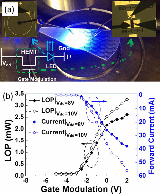
Figure 2: (a) On-testing HEMT-LED emits blue light (inset: circuit schematic). (b) Light output power (LOP) and I–V characteristics of HEMT-LED with modulated gate biases and different Vdd.
The researchers also see possibilities for an LED growth on HEMT integration architecture. The respective methods have different pros and cons. The team comments: “To further boost the development of the monolithic integration of GaN HEMTs and LEDs, growth and fabrication techniques of both architectures need to be investigated for better device performance.”
HKUST HEMTs LEDs AlInGaN GaN MOCVD Sapphire substrates
http://dx.doi.org/10.1063/1.4867235
The author Mike Cooke is a freelance technology journalist who has worked in the semiconductor and advanced technology sectors since 1997.


