


- News
18 March 2014
InP/GaAsSb DHBT with record more than 700GHz power-gain cut-off
The Swiss Federal Institute of Technology (ETH-Zürich) has reported a record power-gain cut-off frequency, fMAX, of 700GHz for a double heterostructure bipolar transistor (DHBT) based on indium phosphide (InP) and gallium arsenide antimonide (GaAsSb) [Ralf Flückiger et al, Appl. Phys. Express, vol7, p034105, 2014].
The epitaxial material structure (Figure 1) was achieved using metal-organic chemical vapor deposition (MOCVD) on 2-inch semi-insulating InP substrates. The heterostructure used staggered gap ‘Type II’ InP/GaAsSb junctions where the band discontinuities are in the same direction. Such structures allow the use of a simplified pure InP collector, giving good thermal conductivity and high breakdown voltages.
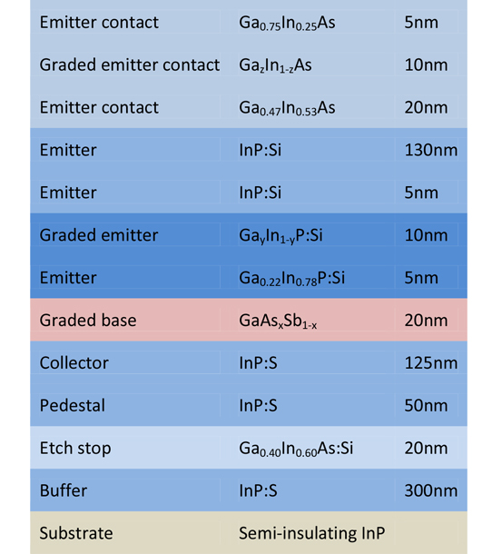
Figure 1: Epitaxial layer sequence. The gradings in the upward direction were x = 0.41-0.59, y = 0.22-0.00, and z = 0.47-0.75.
The transistors were constructed as ‘triple-mesa’ devices with 0.4μm-wide emitter and base, achieved with inductively coupled plasma and wet etch processes. The emitter-base junction area was 0.3μmx4.4μm.
The emitter and base electrodes consisted respectively of titanium/platinum/gold and palladium/nickel/platinum/gold. The surface of the GaAsSb base was treated using an in-situ argon sputtering process before metal deposition (Figure 2). The treatment is found to reduce contact resistivity from ~10-6Ω-cm2 to ~10-9Ω-cm2. The process removed about 10nm of GaAsSb, including oxidation layers. The emitter was protected by the metal contact electrode layers that acted as a self-aligned mask.
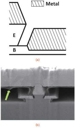 Figure 2: (a) Schematic representation of emitter and base contact. The emitter contact acts as a mask for argon sputtering and protects base access region. (b) Scanning electron micrograph of focused-ion-beam cross section of representative DHBT. Arrow indicates residuals of Teflon planarization.
Passivation of the emitter and base sidewalls was provided by plasma-enhanced chemical vapor deposition (PECVD) of silicon nitride. A low-temperature Teflon-based etch-back process was used to planarize the devices before the deposition of probe pads.
The RF performance was measured between 0.2GHz and 40GHz, giving estimated current- (fT) and power-gain (fMAX) cut-offs of 442GHz and 701GHz, respectively, at a collector-emitter voltage (VCE) of 1.2V. With a higher VCE of 1.6V, the corresponding estimates were 429GHz and 715GHz.
The researchers write: “The present devices show a ~100GHz higher fMAX than those previously reported with the same epitaxial layer structure.”
The DC gain of the device was 11 and the common-emitter breakdown voltage (BVCEO) was more than 5V.
InP and GaAsSb DHBT InP GaAsSb DHBT MOCVD InP substrates
http://iopscience.iop.org/1882-0786/7/3/034105/article
The author Mike Cooke is a freelance technology journalist who has worked in the semiconductor and advanced technology sectors since 1997.


