


- News
5 March 2014
Indium gallium nitride LEDs produced at 480°C
Researchers in Japan have produced working indium gallium nitride (InGaN) semiconductor light-emitting diodes (LEDs) using a low-temperature (480°C) pulsed sputtering deposition (PSD) process [Eiji Nakamura et al, Appl. Phys. Lett., vol104, p051121, 2014].
The team from University of Tokyo and Japan Science and Technology Agency’s CREST fundamental science program is working towards the production of nitride semiconductor LEDs on large-area glass substrates. While traditional GaN device production substrates of sapphire or even silicon are limited to less than 300mm diameter, glass panels are available in sizes of 2m x 2m and more.
However, glass softens above 500°C, well below the conventional metal-organic chemical vapor deposition (MOCVD) growth temperature of ~1000°C.
The Tokyo/CREST team has developed the PSD technique as a way to reduce growth temperatures: “The PSD growth technique has a unique feature of enhanced surface migration of growth precursors due to the pulsed supply of group III metals, which leads to a dramatic reduction in the growth temperature of nitride films.”
All epitaxial layers were grown at 480°C on semi-insulating GaN templates on sapphire substrate. As is often the case with GaN-based devices, the difficult/critical part is finding a suitable methodology for creating p-type (hole) conduction through magnesium (Mg) doping.
At such low growth temperatures, such layers can suffer from incorporation of donor-like native point defects and residual impurities. Tests on Mg-doped GaN on the template were first carried out to optimize the process to bring these problems under control (Table 1). The researchers found that they had to grow the layer under near stoichiometric conditions (i.e. with the Ga and N supply balanced) to achieve p-type conduction.
Table 1: Carrier concentration and mobility of Mg-doped GaN films with different growth stoichiometries.
| Growth condition | Carrier type | Carrier concentration (/cm3) | Mobility (cm2/V-s) |
| Ga-rich | n-type | 1.5x10¹⁹ | 42 |
| Stoichiometric | p-type | 3.0x10¹⁷ | 3.1 |
| N-rich | n-type | 4.7x10¹⁸ | 22 |
In addition, the p-GaN layer exhibited a “clear step and terrace structure” with a root-mean-square (RMS) surface roughness of 0.67nm, as determined by atomic force microscopy (Figure 1). The researchers suggest that the improvement in Mg-doping for near-stochiometric GaN was due to the improved surface morphology and reduction in number of point defects. Temperature-dependent Hall measurements gave an activation energy estimate for the Mg acceptors of 153meV, comparable with values obtain in conventional high-temperature MOCVD.
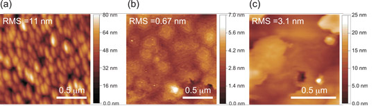
Figure 1: AFM surface images of Mg-doped GaN films grown at 480°C under (a) N-rich, (b) near stoichiometric, and (c) Ga-rich conditions.
Using these results, the researchers attempted to produce LEDs at 480°C with n-GaN, 30nm InGaN, and 300nm p-GaN layers. The indium content of the InGaN was determined to be 0.33, according to x-ray analysis. Temperature-dependent photoluminescence measurements gave a value of 24% for the internal quantum efficiency (IQE).
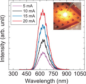 Figure 2: Electroluminescence spectra of LED structure grown at 480°C at forward currents from 5mA to 20mA. Inset: optical image of orange electroluminescence at forward current of 20mA.
Current-voltage measurements showed “good” rectification with a -5V reverse bias current leakage of 3x10⁻⁵A. The clear orange electroluminescence emission wavelength was around 640nm (Figure 2).
Combining the results of this research and a recent demonstration of fabrication of nearly single-crystalline nitride-based LEDs on an amorphous substrate using a graphene buffer layer by the same team, the researchers hope to produce nitride-based LEDs on glass.
InGaN LEDs LEDs InGaN Pulsed sputtering deposition Glass substrates
http://dx.doi.org/10.1063/1.4864283
The author Mike Cooke is a freelance technology journalist who has worked in the semiconductor and advanced technology sectors since 1997.


