


- News
12 March 2014
Direct growth of graphene on aluminium nitride on silicon
Researchers in France have developed a technique to directly grow graphene on aluminium nitride (AlN) crystalline templates on silicon substrates [A. Michon et al, Appl. Phys. Lett., vol104, p071912, 2014].
Up to now, attempts to use graphene in conjunction with III-V semiconductor devices have generally used graphene grown on copper foil that is then transferred to the target application. Another technique to grow graphene is to anneal silicon carbide (SiC) substrates at ~1200°C, driving out the silicon from the surface and leaving the carbon atoms in a graphene structure.
Recently, techniques have been developed for molecular beam epitaxy (MBE) and chemical vapor deposition (CVD) of graphene on silicon carbide and sapphire. The technique developed at CRHEA-CNRS, L2C-CNRS/Université Montpellier 2, and NOVASiC could open up graphene for applications using larger-area and lower-cost production such as for CMOS or for gallium nitride (GaN)-based light-emitting devices and power/high-speed electronic devices.
The AlN template layer was grown using MBE on Si(111) substrates. Monolayer nucleation was performed at 650°C. The temperature was raised to 920°C for the main AlN growth. The target thickness of the template layer was 200nm. The researchers find that their process results in less than 2x10¹¹/cm2 dislocation density with ~30nm crystal grains.
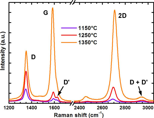
Figure 1: Raman spectra of off-axis AlN/Si(111) templates after graphene growth.
The template material was diced into 1cm2 samples. The graphene was grown in a resistively heated hot-wall CVD system designed for SiC epitaxy. The carbon source was propane (0.17%) in hydrogen/nitrogen (50%/50%) carrier. The carrier gas composition was a balance to avoid the AlN etching effect of hydrogen and the island formation found with high nitrogen concentration. The islands are thought to consist of aluminium droplets. The graphene growth pressure and time were 800mbar and 6 minutes, respectively. Various growth temperatures – 1150°C, 1250°C and 1350°C – were explored.
Atomic force microscopy (AFM) and low-energy electron diffraction (LEED) analysis suggested that graphitic material grown on 2° off-axis templates gave better results than material using on-axis templates.
Raman spectroscopy on off-axis samples showed the presence of defects, especially at lower growth temperatures (Figure 2). The Raman measurements gave estimates of the number of graphene layers as between 1 and 3 for the low-temperature growth (1150°C and 1250°C) and 10 for the high-temperature process (1350°C). The crystallite sizes were around 5-6nm for the lower-temperature growth processes, but around 30nm at 1350°C. The crystallite size at 1350°C seems to be limited by the crystal grains of the AlN templates. The peak shifts of the Raman spectrum indicate a compressive strain in the graphene layers.
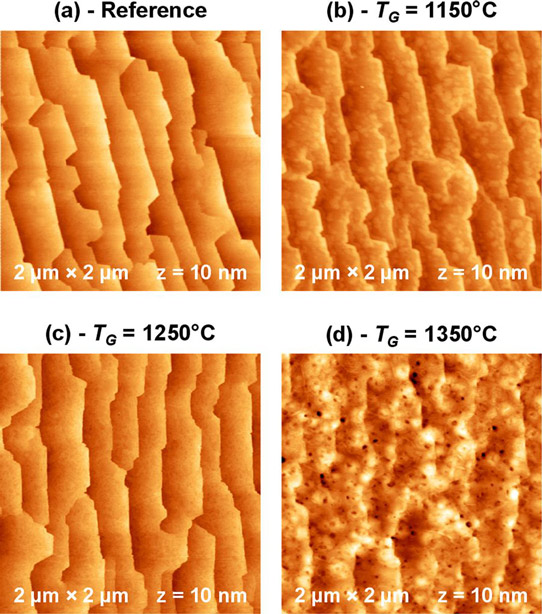
Figure 2: AFM views of off-axis AlN/Si(111) templates after annealing (a) and after graphene growth at 1150°C (b), 1250°C (c) and 1350°C (d).
LEED patterns also suggested some rotational disorder, which can be at least partly attributed to up to 6° rotation of the crystal structure between the grains of the underlying AlN. AFM images of the higher-temperature sample revealed pitting (Figure 2), probably due to an increased etching effect of the hydrogen.
The researchers suggest that “high-quality graphene could be grown on bulk AlN substrates, thanks to a lower density of defects and to the possibility to grow graphene at temperatures above the silicon melting point.”
The researchers also suggest that the process could be used to provide a graphene layer to protect against etching in high-temperature annealing of AlN or other nitride films. “This may be useful for thermal treatment of nitrides films to increase crystalline quality or to activate doping after ion implantation,” they write.
AlN on silicon substrates Graphene GaN SiC substrates CMOS NOVASiC MBE CVD
http://dx.doi.org/10.1063/1.4866285
The author Mike Cooke is a freelance technology journalist who has worked in the semiconductor and advanced technology sectors since 1997.


