


- News
25 March 2014
Improving as-grown indium gallium nitride solar cells
Researchers in France have reported on solar cell devices based on indium gallium nitride (InGaN) multiple quantum wells (MQWs) [Sirona Valdueza-Felip et al, Appl. Phys. Express, vol7, p032301, 2014]. Conversion efficiencies of up to 2% were achieved. Although such values are not commercial, there is interest in developing such structures for inclusion in devices that use multiple junctions to optimize power conversion performance with respect to the solar spectrum.
Sirona Valdueza-Felip of CEA-Grenoble, INAC/SP2M/NPSC, comments: “Our work differs from that of others working on InGaN-based solar cells since we give conversion efficiency values of as-grown structures, meaning that neither top or back coating nor surface treatment has been used; just the contribution of the InGaN/GaN MQW structure is taken into account in the efficiency measurements.
“For example, the excellent results obtained by the group of J. S. Speck at University of California Santa Barbara [http://dx.doi.org/10.1063/1.3591976] achieved conversion efficiencies of 2.29% for solar cells with 30-period QWs with a rough surface under 1 sun of AM1.5 equivalent illumination. However, without roughening the conversion efficiency dropped to 1.33%.”
In addition to CEA-Grenoble, INAC/SP2M/NPSC, the team also included researchers from CEA, LITEN and CNRS-Institut Néel.
The devices (Figure 1) were grown using metal-organic chemical vapor deposition (MOCVD) on sapphire (Al2O3). The silicon-doped n-type gallium nitride (GaN:Si) buffer consisted of 3.2μm with 6x10¹⁹/cm3 carrier density and 10nm heavily doped to 2x10¹⁹/cm3 carrier density. The MQW consisted of 15 or 30 InGaN layers in GaN barriers. The magnesium-doped p-type GaN (GaN:Mg) was doped at 7x10¹⁶/cm3.
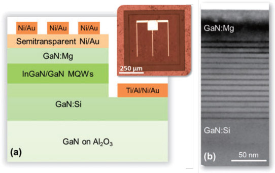
Figure 1: (a) Schematic description of InGaN/GaN MQW solar cell structure. Inset: top-view optical microscopy image of a solar cell with 0.5mm x 0.5mm mesa. (b) TEM image of n-GaN/i-MQW/p-GaN stack (S4 in Table 1).
Four device types with varying structure of MQWs were produced (Table 1). The MQWs with 0.1 indium fraction (x) were grown at 750°C. The more delicate growth with 0.19 In-content was performed at the lower temperature of 720°C.
Table 1: Structural characteristics of InGaN/GaN MQW structures: indium mole fraction in wells (x), number of MQWs, thicknesses of GaN barriers (dB), InGaN wells (dW), and Mg-doped GaN layer (dMg). Electrical performance is given in terms of open-circuit voltage (Voc), short-circuit current density (Jsc), fill factor (FF), and overall conversion efficiency (η).
| Sample | x | Qty of MQWs |
dB (nm) |
dW (nm) |
dMg nm) |
Voc (V) |
Jsc (mA/cm2) |
FF (%) | η (%) |
| S1 | 0.10+/-0.01 | 15 | 8.5+/-0.2 | 1.3+/-0.2 | 60 | 1.5+/-0.1 | 0.13+/-0.01 | 57.8+/-0.1 | 0.11+/-0.01 |
| S2 | 30 | 8.0+/-0.2 | 1.3+/-0.2 | 60 | 2.1+/-0.1 | 0.23+/-0.01 | 58.9+/-0.1 | 0.29+/-0.01 | |
| S3 | 0.19+/-0.01 | 15 | 9.0+/-0.2 | 2.0+/-0.2 | 60 | 1.7+/-0.1 | 3.00+/-0.01 | 39.3+/-0.1 | 2.00+/-0.01 |
| S4 | 30 | 8.8+/-0.2 | 2.0+/-0.2 | 200 | 1.5+/-0.1 | 1.81+/-0.01 | 49.9+/-0.1 | 1.36+/-0.01 |
Devices were fabricated with 0.5mm x 0.5mm and 1mm x 1mm mesas, etched using chlorine-based inductively coupled plasma. The n-GaN ohmic contact consisted of titanium/aluminium/nickel/gold. The p-GaN ohmic contact was a semi-transparent layer of annealed nickel/gold and a nickel/gold electrode grid with 5μm-wide fingers at 150μm pitch.
The spectral cut-offs for MQWs with 0.1 and 0.19 indium content were at wavelengths of 380nm and 465nm, respectively. The values are red-shifted from the 365nm cut-off of pure GaN. Increasing the number of wells from 15 to 30 boosts external quantum efficiency (EQE) by factors of 2-2.5 for either indium content.
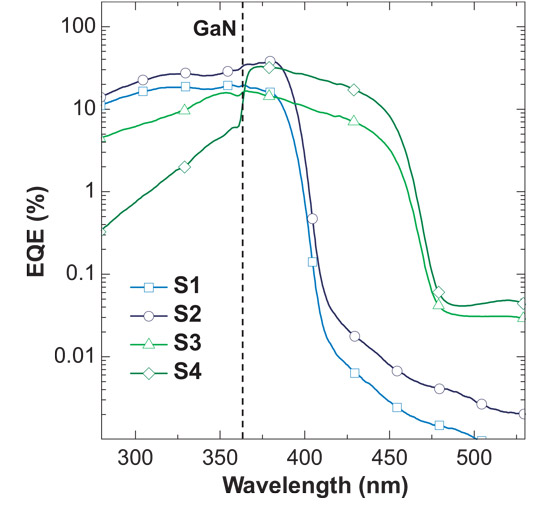
Figure 2: Spectral response of InGaN/GaN MQW samples (S1–S4 in Table 1). The dotted line corresponds to GaN spectral cutoff.
Under 1-sun radiation corresponding to an AM1.5 solar spectrum, the conversion efficiency was highest at 2% for the 15-well 0.19-indium-content device. The lower-indium-content devices suffered from having a shorter wavelength cut-off, while the bulk of the solar spectrum is weighted towards longer wavelengths. However, the higher-indium-content device suffers from ~3x higher series resistance and smaller shunt resistance for blocking leakage. Although the 30-well devices have higher EQE, the advantage is offset by the presence of a 200nm-thick photon-absorbing p-GaN layer (dMg in Table 1) in the case of higher indium content.
InGaN MQWs solar cells InGaN GaN
http://iopscience.iop.org/1882-0786/7/3/032301/article
The author Mike Cooke is a freelance technology journalist who has worked in the semiconductor and advanced technology sectors since 1997.


