


- News
26 June 2014
Developing boron nitride toward deep ultraviolet optoelectronic apps
Professors Hongxing Jiang and Jingyu Lin at Texas Tech University believe that using boron nitride as the p-type contact layers in nitride semiconductor heterostructures “could ultimately pave the way toward the realization of high-efficiency nitride deep ultraviolet (DUV) optoelectronic devices” [Semicond. Sci. Technol., vol29, p084003, 2014].
DUV light-emitting diodes are being developed for spectral analysis, photocatalysis and decontamination/sterilization applications. Present DUV systems involve bulky, fragile and poisonous mercury lamps. A solid-state solution based on aluminium gallium nitride (AlGaN) LEDs is desired but, for the shorter UV wavelengths, external quantum efficiencies plummet to less than 10% at 20mA injection current in the range 270−280nm. For the ~250nm wavelengths needed for effective killing of bacteria and viruses, the efficiency level is a measly 3%.
Jiang and Lin see the most important roadblock in such developments as being the poor p-type hole carrier densities and conductivity of AlGaN at the high aluminium fractions needed for short wavelengths. The magnesium doping used to achieve p-AlGaN has activation energies (500−600meV) – even higher than that of p-GaN (~180meV), which is already a poor performer. High activation energy means low carrier concentrations and hence low conductivity.
A further obstacle in DUV LEDs is that a thin p-GaN layer is added to achieve decent ohmic contact with the metal p-electrode. The DUV photons have sufficient energy to excite electrons from the valence to conduction band and hence these p-GaN layers absorb the light emitted by the active layers, cutting light extraction efficiency.
Jiang and Lin have been exploring the growth of boron nitride in the hexagonal crystal structure (hBN) as an alternative. Although the lattice mismatch between hBN and wurtzite AlN (wAlN) is large at 19.54%, Jiang and Lin noticed that 4x the a lattice constant of wAlN (4x0.3112nm = 1.245nm) is almost equal to 5x the a lattice constant of hBN (5x0.2504nm = 1.252nm). The researchers comment: “This 5/4 coincidence in the hBN/w-AlN heterojunction interface reduces the effective lattice mismatch from 19.54% to about 0.58%.”
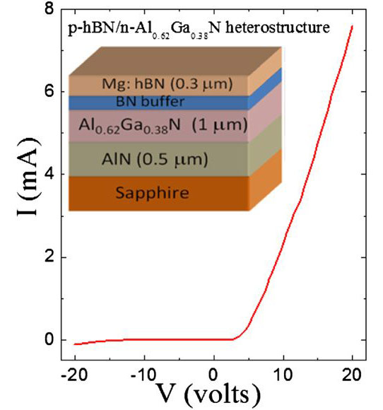
Figure 1: Current versus voltage diode behavior and (inset) schematic illustration of p-hBN/AlGaN/AlN pn structure with p-contacts annealed at 1020°C.
Texas Tech has not as yet reported a DUV LED with h-BN p-contact layer, but pn diodes with “decent” behavior have been demonstrated (Figure 1). Jiang and Lin hope that the use of p-hBN contact layers in DUV LEDs (Figure 2) will enhance hole injection efficiency, more effectively block electrons from entering the p-contact region, reduce contact resistance, and dramatically increase UV transparency for wavelengths longer than 230nm due to the wide ~6eV bandgap of hBN.
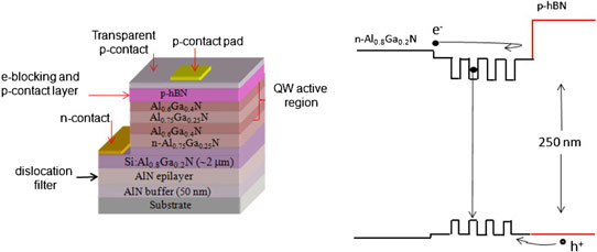
Figure 2: (a) Schematic of DUV LED layer structure proposed by Texas Tech. (b) Energy band diagram of DUV LED layer structure suggests a band alignment that blocks electrons from entering the p-contact region, while posing little barrier to holes entering the active region.
The p-hBN/n-AlGaN diode heterostructures were grown using metal-organic chemical vapor deposition (MOCVD) on sapphire substrates. The p-BN layer used tri-ethyl boron, ammonia and biscyclopentadienyl-magnesium as precursors.
A low-temperature 800°C buffer layer was used to avoid adhesion problems and cracking. The quality of the p-hBN epilayer improved as the buffer was thinned from 140nm to 20nm.
The growth temperature of the hBN epilayer was in the range 1300−1350°C. The hBN layer had an x-ray diffraction (002) rocking curve full-width at half-maximum (FWHM) of 662arcsec – larger than for hBN grown direct on sapphire. This indicates room for improvement in crystal quality.
The p-hBN was activated with an 1150°C anneal for 45 minutes in nitrogen. When grown on an insulating substrate the p-hBN epilayer has demonstrated a 2.3Ω-cm resistivity. The researchers estimate the activation energy at 31meV based on temperature-dependent resistivity measurements.
The present p-hBN epilayers have low mobility (~2cm2/V-s) and free-hole concentrations lower than expected (~1018/cm3 when doped with magnesium concentration of 1019/cm3). The researchers believe that appreciable concentrations of defects may be acting as free-hole compensating centers. The source of the defects is presently unclear. Clarification should lead to larger carrier concentrations and higher mobility.
The pn diode was achieved with an inductively coupled plasma (ICP) etch to expose the n-type AlGaN layer. The n-contact metals consisted of annealed titanium/aluminium/nickel/gold. The p-contact was nickel/gold. The p-contact was annealed in a variety of conditions, but full characterization of the ohmic contact resistance and comparison with p-GaN remains to be performed. With 1020°C annealing of the p-hBN/metal contact, the reverse bias leakage at −10V was 3μA.
http://dx.doi.org/10.1088/0268-1242/29/8/084003
The author Mike Cooke is a freelance technology journalist who has worked in the semiconductor and advanced technology sectors since 1997.


