


- News
19 June 2014
Stress bumps improve nitride semiconductor packaged transistor performance
Researchers in Taiwan claim to be the first to use bumping technology to create piezoelectric-induced performance enhancement in flip-chip packaged aluminium gallium nitride (AlGaN) high-electron-mobility transistors (HEMTs) [Szu-Ping Tsai et al, IEEE Electron Device Letters, published online 29 May 2014]. Such HEMTs are being developed for high-power switching devices for automotive, cell-phone base-station system and phased-array radar applications.
AlGaN HEMTs depend on the polarization fields in the buffer GaN and barrier AlGaN to create the two-dimensional electron gas (2DEG) channel in the buffer near the barrier. These polarization fields arise as a result of the ionic nature of the bonds between the elements in the compound. The nature of the polarization field is affected by the stress state of the material, giving opportunity to improve performance through piezoelectric effects.
Some researchers have used external means to produce strain in nitride semiconductor HEMTs to enhance performance, but the team based at National Chiao Tung University and Yuan Ze University decided to use the bumping process that is used in flip-chip packaging as a means to introduce stress.
Six different bump patterns were designed on AlN substrates (Figure 1) consisting of electroplated gold. Various forms of bump were used: circular cylinders of 25μm and/or 10μm radius and 25μm height, and/or various rectangular bumps. The ‘optimized’ design (Figure 1f) used six rectangular bumps on the source fingers, giving a 500μm length and 18μm width. The optimized design also had rectangular bumps covering the contact regions of the device.
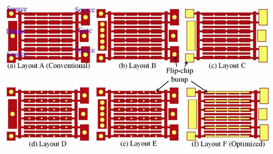
Figure 1: Layouts of six different bump patterns on AlN substrate.
The researchers comment: “These bump patterns were designed to induce increasing levels of tensile stress, with the optimized case giving the highest strain, as verified through numerical simulations.”
The stress was designed to arise in the thermal bonding process as a result of the different coefficients of thermal expansion of gold (14.2 parts per million/°C) and GaN (5.6ppm/°C).
The HEMT heterostucture was grown by metal-organic chemical vapor deposition (MOCVD) on 1000μm-thick silicon substrate. The heterostructure consisted of a 120nm AlN buffer, 5.5μm GaN channel, 25nm AlGaN barrier, and 4nm GaN cap. The transistors consisted of 10-finger structures with 2μm gate length and 500μm gate width.
In DC measurements, the maximum drain current of the bare 5mm die was 850mA. In flip-chip packaged form the drain current for the optimized case exceeded the DC-mode 1A limit of the Agilent B1505A power device analyzer. However, this result does not reveal the strain effect, since the improvement is largely due to the improved thermal dissipation of the packaged device through the flip-chip bumps compared with the bare die.
To separate out the strain effect, the researchers performed pulsed measurements to avoid self-heating (Figure 2). The current ‘improvement’ over the bare die ranged from −12.7% (i.e. worse than bare die) for the conventional bump layout to +4.3% for the optimized bump design – a range of 17 percentage points. Relative to the conventional bump packaged device, the optimized bumping scheme improved the current by 19.5% (104.3/(100-12.7) = 1.195).
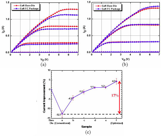
Figure 2: Pulsed measurements of drain current versus voltage for FC-bonded AlGaN/GaN HEMTs with (a) conventional bump pattern and (b) optimized bump pattern. (c) Improvements relative to bare die of maximum drain current for six different FC package bump layouts.
The researchers also found a slight negative shift of threshold voltage (~3%) with optimized strain. This is attributed to the induced piezoelectric effect, which leads to an increase in the sheet carrier density.
Flip-chip technology AlGaN HEMTs AlGaN GaN AlN substrates MOCVD
http://ieeexplore.ieee.org/xpl/articleDetails.jsp?arnumber=6823098
The author Mike Cooke is a freelance technology journalist who has worked in the semiconductor and advanced technology sectors since 1997.


