- News
13 June 2014
MicroSense ships LED sapphire wafer measurement tools for process control
MicroSense LLC of Lowell, MA, USA, which supplies dimensional non-contact wafer metrology equipment for manufacturing silicon, compound semiconductor and power devices as well as magnetic metrology systems for MRAM (magnetoresistive random-access memory) manufacturing, has announced multiple shipments of its new, next-generation UltraMap C200 automated sapphire wafer metrology tool.
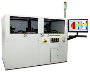
 Picture:
MicroSense’s UltraMap C200A automated LED sapphire wafer measurement system.
Designed specifically for high-throughput dimensional measurement of sapphire wafers for LED manufacturing, the UltraMap C200 provides throughput of 90 x 6”-diameter sapphire wafers per hour with what is reckoned to be low cost of ownership (CoO). The system uses MicroSense’s proprietary two-sided capacitive sensing technology to measure sapphire wafer geometry, including thickness, TTV (total thickness variation), bow, warp, and LTV (local site thickness variation).
“LED manufacturers typically don’t make their own sapphire wafers, so incoming quality control has become a requirement for LED chip makers as the industry continues to migrate from primarily 2” wafers to 4”, 6” and 8” wafers,” says David Kallus, director of Dimensional Wafer Metrology at MicroSense. “LED manufacturers have found high sapphire wafer bow strongly correlates to LED yield loss. The UltraMap C200 utilizes our proprietary capacitive sensing technology and advanced high-density wafer mapping algorithms to provide world-leading measurement repeatability and throughput,” he claims.
“Sapphire factories are scaling to capacities unheard of before, driven by the LED and smartphone component markets,” says Kallus. “In order to improve sapphire wafer yields and drive down wafer cost, wafer manufacturers need to measure at more steps in the wafering process,” he adds. “Unlike metrology tools based on optical methods, the MicroSense UltraMap C200 measures sapphire wafers and substrates with any surface finish – as-cut, lapped, ground, polished, textured and patterned sapphire substrates (PSS) – without sacrificing wafer throughput or measurement repeatability,” Kallus claims. “Wafer surface condition has no effect on measurement performance.”
Capable of handling wafers of 2-8” in diameter, the UltraMap C200 is available in three versions, including tools with robotic loading, robotic loading with cassette sorting, and a bench-top tool.
MicroSense's latest developments in sapphire wafer metrology, MRAM wafer metrology and high-resolution capacitive sensors will be on display in booth 2143 South Hall in the Moscone Center at the SEMICON West 2014 show in San Francisco (8-10 July).
Metrology firm MicroSens acquires SigmaTech


