


- News
3 June 2014
Electrically pumped light emission in germanium on silicon substrates
Chinese Academy of Sciences Institute of Semiconductors has been studying a lateral light-emitting diode (LED) and waveguide structure based on germanium [Zhi Liu et al, Appl. Phys. Lett., vol104, p191111, 2014].
Like silicon (SΓΓi), germanium (Ge) is an indirect-bandgap semiconductor, which means that creating the conditions for efficient light emission should be very difficult. However, the band structure of Ge has a direct ‘gamma’ (Γ) valley in the conduction band that has a gap from the valence band only ~140meV wider than the indirect gap of ~660meV. By contrast, Si has an indirect gap of 1.12eV (the 6 ‘chi’ or Χ valleys) and a direct Γ gap of 3.4eV.
The small difference between germanium’s indirect and direct transitions raises the possibility for ‘pseudo-direct’ light emission through tweaking the band structure with strain and/or filling/doping the 4 indirect ‘L’ valleys so that the Γ valley can become populated with electrons.
Fabricating effective Ge light-emitters would have benefits for optoelectronics based on Si waveguides and silicon CMOS, since Ge and SiGe alloys are already integrated in Si transistor mass-production processes.
The germanium film was grown on lightly doped n--silicon (n--Si) substrates by cold-wall ultra-high-vacuum chemical vapor deposition (UHV-CVD). The precursor was pure germane (GeH4). The 60nm buffer layer was grown at 290°C, and the main 740nm Ge layer at 600°C.
A 300nm silicon dioxide (SiO2) film was grown by plasma-enhanced CVD (PECVD). The wafer was then annealed rapidly to improve crystal quality and to create tensile strain of between 0.20% and 0.22%. The Ge film was formed into 1μmx350nmx0.5mm ridge structures, with the SiO2 forming a mask for the patterning process.
The regions by the ridge without SiO2 mask were implanted with phosphorous and boron to create n- and p-type regions, respectively. The dopants were thermally activated and the SiO2 mask removed. Between these steps a dilute solution of hydrogen peroxide and hydrochloric acid was used to smooth the sidewalls of the ridge. A new 700nm SiO2 layer was applied using PECVD.
The metal electrodes were created and thermally activated for a good ohmic contact with the Ge film. The structures were cleaved across the <001> facet with waveguide lengths between 0.6mm and 1.3mm.
Using a lateral structure avoids the current having to cross the defect-infested region of the Si/Ge interface. The researchers comment: “The device exhibited a good rectifying behavior and had excellent injection efficiency. The current density was about 100 kA/cm2 with a 2V forward bias.”
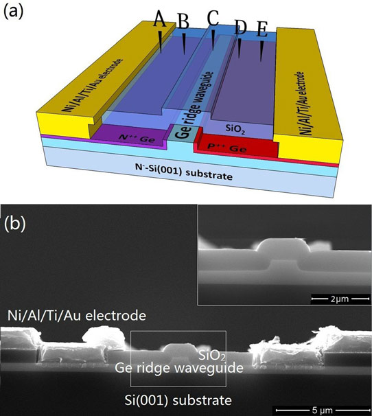
Figure 1: (a) Schematic of Ge p-i-n ridge waveguide LEDs on Si substrate. Top surface positions marked A to E for micro-electroluminescence measurement are shown. (b) Cross-sectional SEM of Ge p-i-n ridge waveguide LEDs and cleaved facet. Top width and height of the ridge waveguide are 900nm and 350nm, respectively.
The waveguide peak emission wavelength of 1625nm at 30kA/cm2 injection current was significantly red-shifted compared with the 1590nm photoluminescence of 0.21% tensile-strained undoped Ge. The researchers suggest the red-shift could be due to self-heating caused by the high injection current. The bandgap tends to shrink at high temperature. The halting of the red-shift trend beyond 110kA/cm2 is attributed to the low energy cut-off of the InGaAs detector used. Under 150kA/cm2 current injection, the light output power was around 1μW.
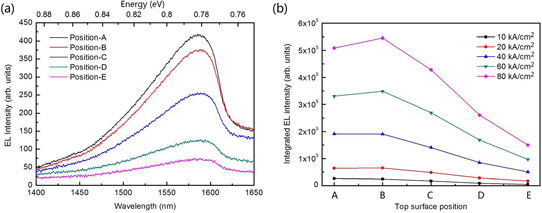
Figure 2: (a) Room-temperature top surface micro-electroluminescence spectra at various surface positions (Figure 1a) of Ge waveguide LED with fixed current density of 10kA/cm2. (b) Integrated top surface EL intensities at different top surface positions (A-E) with varying current density.
The researchers also studied the emission from the top surface with a microscope at 10kA/cm2. The emission peak in this case was 1587nm, consistent with the peak for 0.21% tensile-strained undoped Ge. The amount of emission was greatest near the n-contact region (position ‘A’ in Figure 1). The direct-transition ‘Γ’ valley is more likely to be populated near the n-type region than in the p-type region. As the current increases, the maximum emission region moved nearer to the intrinsic region.
The researchers believe that their results indicate the potential of Ge as a Si-based light-source.
Lateral LEDs Germanium PECVD Si substrates
http://dx.doi.org/10.1063/1.4878619
The author Mike Cooke is a freelance technology journalist who has worked in the semiconductor and advanced technology sectors since 1997.


