


- News
29 July 2014
Aspect ratio trapping to improve InGaAs quality on silicon
Researchers based in France and USA have been working on ways to improve material quality for indium gallium arsenide (InGaAs) compound semiconductor quantum wells (QWs) on silicon (Si) [R. Cipro et al, Appl. Phys. Lett., vol104, p262103, 2014]. The researchers from Université Grenoble Alpes, Université de Lyon, and US-based Applied Materials are seeking ways to incorporate III-V high-mobility materials on silicon and thus boost transistor performance.
One of the main problems with growing InGaAs and related materials on silicon is lattice mismatch, with differences of 4% for pure GaAs and 11% for InAs, respectively, compared with silicon. Often, the materials are grown on indium phosphide (InP) substrates and transferred by complex direct wafer bonding techniques. Direct growth on silicon would be preferable.
Instead, the researchers used an ‘aspect ratio trapping’ (ART) method, where the compound semiconductor material was grown in trenches in silicon dioxide (SiO2) on 300mm Si (100) in an Applied Materials metal-organic chemical vapor deposition (MOCVD) system. The trenches were aligned in the [110] direction. The growth of the compound semiconductors was preceded by cleaning using Applied’s SiCoNi technology developed for cobalt/nickel physical vapor deposition (PVD).
A GaAs nucleation layer was grown directly on the exposed silicon surface at low temperature, followed by higher-temperature growth (less than 550°C) of GaAs/AlAs/InGaAs/AlAs/GaAs. The aluminium arsenide (AlAs) constituted the barrier parts of the QW system.
The researchers were particularly keen to remove anti-phase boundary (APB) defects. With just 180nm GaAs grown in the trenches, the APB density was found to decrease as the width of the trench decreased. The APB density estimated from micro-photoluminescence measurements was 3.9/μm with 1000nm trench width (0.18 aspect ratio). This reduced to 0.25/μm with 300nm trenches (0.6 AR).
The researchers add: “For narrower cavities, APBs are no longer observed. An aspect ratio of 1.3 is sufficient to completely annihilate the APBs.”
Scanning transmission electron micrographs (STEM) of GaAs in 1.3 AR trenches suggested that misfit dislocations beginning at the Si/GaAs interface were blocked by the SiO2 sidewalls and did not proceed vertically through the GaAs layer. TEM study showed that the crystalline defects generated by the 4% GaAs/Si(100) lattice mismatch were confined to the first 20nm of GaAs.
Having developed a good-quality GaAs buffer, the researcher added a GaAs/AlAs/InGaAs/AlAs/GaAs stack to give the InGaAs QW. Secondary-ion mass spectroscopy (SIMS) was used to characterize the abruptness of the interfaces. The interface widths for AlAs/InGaAs, as measured by indium concentration varying from 14% to 86% of maximum, were 2.5nm and 2.9nm for the upper and lower interfaces, respectively.
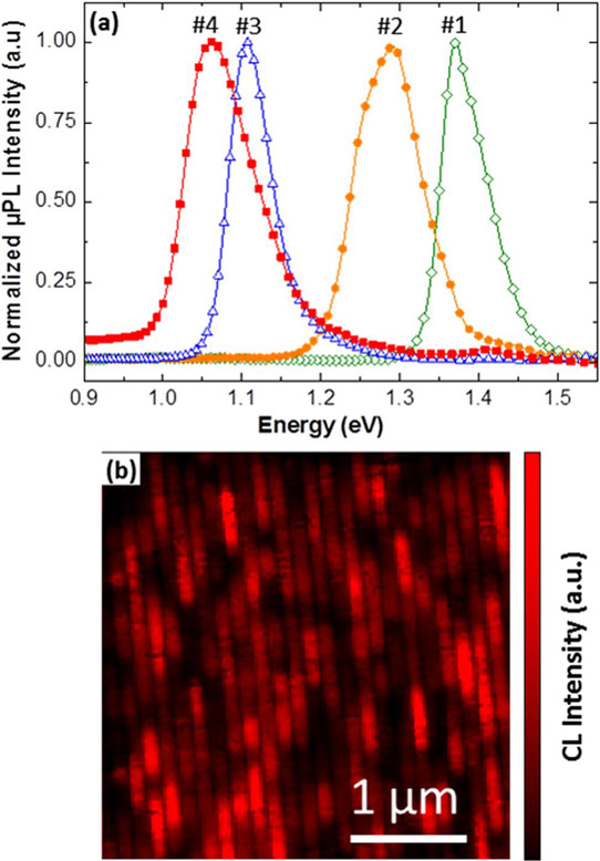
Figure 1: (a) Normalized room-temperature micro-PL spectra of different InGaAs QWs having different composition of indium of (#1) 10%, (#2) 20%, (#3) 30%, and (#4) 40%. (b) 5K panchromatic CL mapping of sample #1.
The InGaAs quantum wells were characterized using micro-PL with 623.8nm excitation from a helium-neon laser. The spot size was 0.5μm. Samples with low-AR trenches (<1.3) did not give any micro-PL signal. The researchers therefore studied only the 1.3 AR materials in depth (Figure 1). There was also a lesser signal from the GaAs layer for band-to-band emission at 1.43eV with a full-width at half maximum (FWHM) of 50meV. The QW emissions varied with indium content (Table 1). The FWHMs of the signals were around 60meV.
Table 1: Characteristics of the samples studied in this work by micro-PL.
| Sample | Targeted In content (%) | Measured InGaAs thickness (nm) | Micro-PL peak energy (eV) | FWHM (meV) | Extracted In content (%) |
| #1 | 10 | 15 | 1.37 | 68 | 7 |
| #2 | 20 | 13 | 1.29 | 95 | 16 |
| #3 | 30 | 10 | 1.10 | 60 | 35 |
| #4 | 40 | 8 | 1.06 | 100 | 42 |
The researchers comment: “The ART strategy combined with an ultra-thin 150 nm GaAs buffer layer seems efficient to block most of the defects such as dislocations and antiphase boundaries. It has been shown that an aspect ratio of 2 is required to effectively suppress the defects in selective epitaxy. But even in our below 1.5 aspect ratio patterns, defect densities are strongly decreased, leading to a room-temperature photoluminescence.”
Cathodoluminescence from an electron beam showed bright and dark zones, suggesting the presence of the dislocations that form non-radiative recombination centers. “Further work is in progress to adapt the cavity aspect ratio and size, and the growth parameters, in order to block the remaining defects and to form defect free QWs,” the researchers say.
The researchers believe that their results are promising for the development of InGaAs nMOSFETs on silicon. Also, due to the relatively low process temperatures, the technique could allow the development of co-integration of germanium-based pMOSFETs to give complementary metal-oxide semiconductor (CMOS) circuitry.
InGaAs InGaAs on silicon Aspect ratio trapping MOCVD InGaAs nMOSFETs
http://dx.doi.org/10.1063/1.4886404
The author Mike Cooke is a freelance technology journalist who has worked in the semiconductor and advanced technology sectors since 1997.


