


- News
2 July 2014
Pushing deep ultraviolet diodes to higher efficiency
A team of researchers based in the USA has described two of the main developments that has allowed them to achieve external quantum efficiencies of greater than 10% for deep ultraviolet (DUV) light emitting diodes (LEDs) [Max Shatalov et al, Semicond. Sci. Technol., vol29, p084007, 2014]. The team is associated with Sensor Electronic Technology Inc (SETi), US Army Research Laboratory, and Rensselaer Polytechnic Institute (RPI).
The researchers comment on one aspect of their work: “Large-chip LEDs with the output power >75mW CW at 300mA pave the way for DUV semiconductor sources to be used in disinfection, decontamination, curing and medical applications.”
SETi is on its third generation of DUV LEDs, achieving about 10% external quantum efficiency (EQE) and 4.5% wall-plug efficiency (WPE) at 20mA injection in the 270-280nm wavelength range (Figure 1). To achieve improvement over previous generations the researchers focused on reducing the effect of non-radiative (NR) defects and decreasing optical losses in p-GaN contact layers and through the refractive index mismatch between the device material and air.
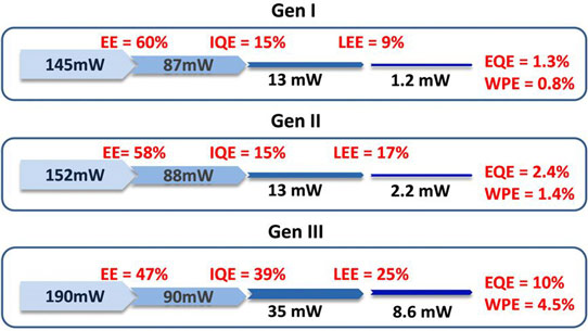
Figure 1: Efficiency and loss mechanisms in small-die DUV LEDs at 20mA drive current.
The problem with p-GaN contact layers arises because the activation energy of the magnesium (Mg) p-type doping increases drastically as more aluminium is introduced in p-AlGaN, reducing the effectiveness of such layers as the means to inject holes into the active region of the LED. UV LED structures therefore usually have a p-contact structure with a combination of AlGaN and pure GaN. Unfortunately, the bandgap of GaN is narrower than the energy of the DUV photons produced in the active region – hence, the p-GaN layer absorbs the radiation and reduces the light extraction efficiency.
The more recent SETi devices use a short-period superlattice (SPSL) of various compositions of p-AlGaN. The technology was first developed for less challenging UV-A (400-315nm) and UV-B (315-280nm) devices and then the Al-content was increased to cross the border into UV-C (280-100nm). Factors that can be adjusted to improve performance include reducing the SL period and tuning the well/barrier compositions to align the hole ground state in the well with the acceptor level in the barrier.
At 275nm, the normal incidence optical transmission can be increased to more than 60% for a p-SPSL, compared with 5% for p-GaN contact layers. Unfortunately, the higher activation energy of the Mg acceptors in AlGaN leads to a higher operating voltage that reduces WPE at high current in small-area devices.
SETi has also developed metal stack reflectors on the p-contact in its Gen II devices with 70% normal incidence reflectivity in the UV region. The researchers attribute a near factor of two improvement in light extraction efficiency (LEE) and EQE to the use of a metal reflector.
Reduced threading dislocation density (TDD) has been achieved through the application of migration-enhanced metal-organic chemical vapor deposition (MEMOCVD) on sapphire with AlN buffer layers. The use of MEMOCVD to create heterostructures with AlGaN/AlN superlattice transition layers between the buffer and device layers has reduced TDD from 5x10⁹/cm2 (Gen I/II) to 2x10⁸/cm2 (Gen III). The transition layer minimizes relaxation and avoids cracking of AlGaN layers grown over AlN templates.
The researchers believe further improvements in material quality can be achieved through growth parameter optimization to alter point defect concentration, quantum well interface sharpness, and alloy composition uniformity.
The use of low-TDD AlN templates (2x10⁸/cm2) allowed the researchers to achieve EQE values of more than 10% in Gen III devices (Structure B, Figure 2). This doubles the EQE of 5% achieved with Gen II devices using higher-TDD templates (3-5x10⁹/cm2) along with LEE enhancements such as surface roughening and encapsulation (Structure A). An intermediate 5x10⁸/cm2 TDD large-area device (Structure C) suffered from LEE problems due to optical losses in the p-SPSL contact region and absorption by the n-contacts.
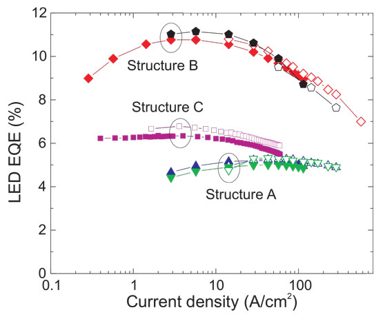
Figure 2: EQE versus current density of LED devices from structures A, B and C under CW (closed symbols) and pulsed (open symbols) pumping.
The lower TDD structures B and C also exhibited earlier onset of efficiency droop at ~5A/cm2 current density, compared with ~50A/cm2 for structure A. The researchers suggest that the efficiency droop could be due to the delocalization of free carriers at higher current densities. With higher defect densities the carriers can be bound to certain regions, inhibiting their migration to non-radiative recombination centers, delaying efficiency droop.
The large-area device based on Structure C achieved continuous wave (CW) 275nm wavelength output powers of 27mW and 75mW at 100mA and 300mA, respectively. The corresponding EQEs were 6% and 5.5%. Using pulsed operation to avoid self-heating effects increased the output power at 300mA to 80mW. At 100mA current, the forward voltage was less than 7V, giving an electrical efficiency of ~60%.
The researchers comment: “It is evident that, for the large-chip devices, use of SPSL top layer is more beneficial since the p-contact and the p-layer voltage drop contribution into the operating voltage is not as strong as in small-chip devices.”
http://dx.doi.org/10.1088/0268-1242/29/8/084007
The author Mike Cooke is a freelance technology journalist who has worked in the semiconductor and advanced technology sectors since 1997.


