


- News
3 July 2014
Enkris uses Aixtron system to demo high-voltage GaN HEMT structures on 200mm silicon
Enkris Semiconductor Inc of Suzhou, Jiangsu, China has demonstrated the manufacture of high-voltage gallium nitride high-electron-mobility transistor (HEMT) structures on 200mm silicon (GaN-on-Si) using a metal-organic chemical vapor deposition (MOCVD) system from Aixtron SE of Aachen, Germany. Enkris’ main products are GaN epiwafers for electronics applications including both wireless communications and high-voltage power switching devices.
GaN-on-Si power devices have attracted much attention from both academics and industry because of their potential applications in power electronics, says Aixtron. Due to the defective nature of heteroepitaxial GaN layers grown on silicon, GaN-on-Si power devices have suffered from high buffer leakage. Most recently, Enkris has produced high-voltage GaN HEMT materials on 200mm silicon with what is said to be excellent uniformity and low buffer leakage combined with thickness uniformity of <0.5% without edge exclusion. Under special conditions, the uniformity value can be improved even further, it is reckoned.
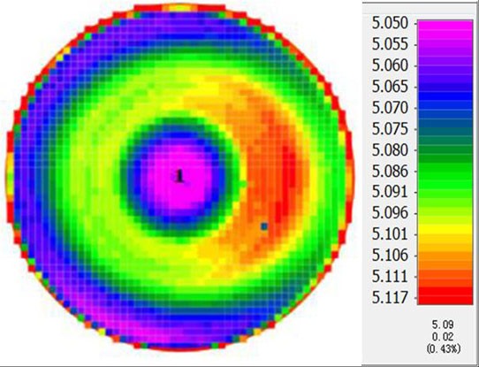
Figure 1: Thickness mapping of 200mm GaN-on-Si wafers.
“It has been well accepted that GaN on large-size silicon substrates is the most cost-effective way to achieve high-volume production of GaN power devices. However, a large wafer bow combined with a high buffer leakage has hindered the further development of the GaN-on-Si technology so far,” says Enkris’ co-founder Dr Cheng Kai. “Our process on 200mm silicon substrates shows that high breakdown voltage (less than 1600V) GaN power devices with low leakage currently can be achieved with relatively thin buffer layers of 4µm. They simplify the growth process, minimize the wafer bow and reduce the epi-cost significantly,” he adds. “Based on our processes, which were applied on an Aixtron system, GaN-on-Si power devices may reach even higher voltages in the near future,” Kai reckons.
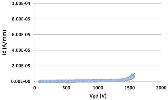
Figure 2: Current leakage of devices fabricated on 200mm GaN-on-Si.
“Enkris’ remarkable success in achieving excellent layer quality and material properties show the capability of our technology for high-voltage GaN HEMT applications,” says Dr Frank Wischmeyer, vice president Power Electronics at Aixtron. “Our MOCVD technology is enabling the integration of wide-bandgap semiconductors on large-diameter silicon substrates,” he adds. “Aixtron is committed to support the power electronics industry advancing toward high-volume 200mm GaN-on-Si device manufacturing.”
Aixtron MOCVD GaN HEMTs on silicon


