


- News
21 January 2014
New ‘universal’ method for transparent conduction on nitride semiconductors
Researchers based in Korea and USA believe they have developed “a universal method of producing transparent electrodes with high conductivity and high optical transmittance in the UV regimes using electrical breakdown (EBD) to form conducting filaments (CFs) providing a current path between the transparent conducting electrodes (TCEs) and the semiconductor, which leads to a large reduction in their contact resistance.” [Hee-Dong Kim et al, Adv. Funct. Mater., published online 11 November 2013].
The team from Korea University, LG Advanced Research Institute, and Rensselaer Polytechnic Institute (RPI) comment: “We highly expect that the proposed CF-based TCEs can be immediately applied to many types of optoelectronic devices (and systems), including LEDs, organic LEDs, solar cells, and even large-area display panels that require TCEs with high conductivity and high transmittance in the UV-to-IR wavelength regimes.”
In particular, the researchers see applications in the deep ultraviolet (DUV), where traditional TCEs such as indium tin oxide (ITO) cut-off. DUV LEDs are being developed as light sources for killing microbes – an application that needs wavelengths shorter than 254nm. Such devices presently have external quantum efficiencies (EQE) of less than 11%.
A further factor reducing EQE in these short-wavelength LEDs is that the p-contact is usually made from p-type gallium nitride (p-GaN), which also absorbs DUV strongly. Ideally one would use an aluminium gallium nitride (AlGaN) layer that has a suitably wide bandgap, transmitting DUV radiation. Unfortunately, AlGaN is difficult to dope in a p-type direction and there has been no work thus far in creating suitable ohmic TCEs.
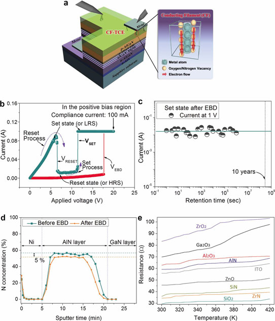
Figure 1: (a) AlGaN-based UV LED schematic after EBD and atomic level view of CF within TCE. (b) Current–voltage characteristics for 80nm AlN TCE on p-GaN before and after EBD through nickel. (c) Retention characteristics of set state at 1V as function of time. (d) Nitrogen concentration of AlN film and the interface between AlN TCE and the p-GaN layer before and after EBD, analyzed by AES. (e) Temperature-dependent resistance characteristics of ITO, Al2O3, ZnO, Ga2O3, ZrO2, SiO2, ZrN, SiN, and AlN TCEs on p-GaN after EBD in 300–420K temperature range.
The researchers used the method to create ohmic or near-ohmic contacts between a range of TCE candidates and p-GaN and p-AlGaN layers. The ohmic connection between the TCE material and underlying p-AlGaN was created using the EBD forming process through applying a relatively large bias of around 17.5V between two nickel electrodes that were placed on the TCE (Figure 1a). The increased conductivity is attributed to the formation of CFs of oxygen or nitrogen vacancies in the material. The technique seems to work with a wide variety of oxides and nitrides.
With aluminium nitride (AlN) on p-type gallium nitride (Figure 1b), a soft breakdown is seen, with the material switching between high- and low-resistance states (HRS/LRS). After a first sweep between 0V and 20V, which switched to the LRS at 17.5V (VEBD), a second sweep showed increased current up to 6.5V (VRESET) and then switched back to the HRS. The LRS was regained by a switch at 12V (VSET).
Of course, with a soft breakdown such as this, one is concerned about retention of the low-resistance state (Figure 1c). The researchers estimate that a bias of 1V giving a current of 18mA could be stably maintained at room temperature for 3x10⁸ seconds (a period of time better known as 10 years). Stability in the LRS was maintained even with 1-1000 second pulses up to 5V.
Auger electron spectroscopy (AES) confirms a depleted nitrogen fraction by about 5%, as would be expected from the formation of CFs after EBD (Figure 1d). Near the GaN layer the depletion is even more apparent, “which facilitated the formation of Ohmic contact between the TCEs and the p-GaN layers.”
The EBD process results in a metallic-like conduction that shows increased resistance at higher temperatures (Figure 1e). The other materials tested showed a similar transition from a non-linear HRS to a ‘perfect’ linear/ohmic LRS after EBD with a similar voltage sweep. Before EBD the 1V current is around 10-9A (1nA), while after EBD the ohmic behavior leads to ~10mA (~10-2A) at the same voltage. The transfer length method (TLM) metal pads for the resistance measurement were separated by 2μm.
The same set of materials was also deposited on p-Al0.5Ga0.5N and subjected to EBD. In this case some of the materials were non-ohmic after EBD. Also, for those that became ohmic, the specific contact resistance was not as low as in the case of p-GaN (Table 1). Even so, the production of ohmic contacts on p-AlGaN has not been tried before because of the challenges of the material such as surface oxidation, poor doping ability for p-type conduction by magnesium, and large workfunction. The 1V current was ~5nA before EBD and ~0.1mA after.
In structures with an AlGaN top layer, a GaN cap is usually applied to protect against oxidation. However, in deep UV devices such cap layers absorb radiation, reducing device efficiency severely.
Table 1: Average specific contact resistance, between TCEs and the p-GaN/AlGaN layers.
| Material [bandgap] | Average specific contact resistance [Ω-cm2] | |||
| on p -GaN | on p -AlGaN | |||
| Before EBD | After EBD | Before EBD | After EBD | |
| ZrN [2.8 eV] | Non-Ohmic | 4.91x10⁻⁵ | Non-Ohmic | Non-Ohmic |
| ZnO [3.1 eV] | Non-Ohmic | 2.81x10⁻⁵ | Non-Ohmic | Non-Ohmic |
| ITO [3.8 eV] | Non-Ohmic | 8.68x10⁻⁵ | Non-Ohmic | Non-Ohmic |
| Ga2O3 [4.8 eV] | Non-Ohmic | 7.56x10⁻⁵ | Non-Ohmic | 2.42x10⁻² |
| SiN [5.6 eV] | Non-Ohmic | 1.01x10⁻⁵ | Non-Ohmic | 2.55x10⁻² |
| ZrO2 [5.8 eV] | Non-Ohmic | 4.79x10⁻⁴ | Non-Ohmic | 2.75x10⁻¹ |
| AlN [6.2 eV] | Non-Ohmic | 2.41x10⁻⁵ | Non-Ohmic | 4.55x10⁻³ |
| Al2O3 [7 eV] | Non-Ohmic | 5.67x10⁻⁵ | Non-Ohmic | 7.10x10⁻³ |
| SiO2 [8.9 eV] | Non-Ohmic | 1.99x10⁻⁵ | Non-Ohmic | 4.55x10⁻³ |
Another factor is that the ‘ohmic’ behavior on p-AlGaN is not ‘perfect’. The researchers write: “Although a perfect Ohmic behavior similar to that observed in the p-GaN layers has not been obtained yet for the p-AlGaN contact layers (probably because of the still immature technology of heavily doped p-AlGaN layers), the obtained result is not only a first-time demonstration of the direct Ohmic contacts in p-Al0.5Ga0.5N layers but also a critical turning point in delivering a technical breakthrough in deep UV LEDs.”
The measured specific contact resistances on GaN are of the order 10-5Ω-cm2. The researchers comment “These values are comparable with (or lower than) the best result reported from the metal-based p-GaN electrodes, with the additional benefit of high transmittance of over 95% at 365nm.”
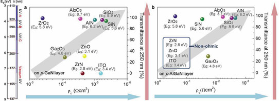
Figure 2: Correlation between contact resistance (ρc) for TCEs on (a) p-GaN and (b) p-Al0.5Ga0.5N after EBD and transmittances at 250nm.
Transmittance characteristics were obtained by depositing the materials on quartz substrates (Figure 2). The transmittance of most of the materials was ~95%, including substrate, across the deep UV to infrared (220nm-800nm) range. The exceptions were bandgap-limited ITO, ZnO, and ZrN.
http://dx.doi.org/10.1002/adfm.201301697
The author Mike Cooke is a freelance technology journalist who has worked in the semiconductor and advanced technology sectors since 1997.


