


- News
27 January 2014
Enhancing silicon carbide epitaxy with high-speed rotation
Researchers in Japan have developed a single-wafer-type 150mm vertical 4H polytype silicon carbide (SiC) epitaxial reactor with high-speed wafer rotation [Hiroaki Fujibayashi et al, Appl. Phys. Express, vol7, p015502, 2014]. The team comments on the results: “The obtained growth rates and doping uniformity for 150mm-diameter wafers are much superior to those reported previously.”
The research team involved collaboration between Central Research Institute of Electric Power Industry, DENSO Corp, NuFlare Technology Inc, Toyota Motor Corp, and Toyota Central R&D Labs.
Although SiC has been developed for high-voltage and low-loss power devices for many years, the commercial impact of the material has been slow because it is expensive and difficult to work. In particular, epitaxial process temperatures are very high, at around 1600°C, compared with 1000°C for gallium nitride and silicon, and 700°C for gallium arsenide and other III-V materials.
SiC-based Schottky diodes have been available commercially since 2001 but, to compete with silicon production, processes need to be higher throughput and need to result in higher-quality epilayers.
The researchers developed a reactor (Figure 1) based on the silicon epitaxy HT-2000 system developed by Toshiba and NuFlare in the 1990s. For SiC, the researchers added extra upper heaters with respect to the lower heaters of the silicon tool.
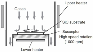 Figure 1: Schematic cross section of epitaxial reactor.
The lower heaters were divided into inner and outer zones, allowing temperature control in the radial direction. The upper heaters were designed for rapid heating of the hot zone to the 1600–1650°C needed for SiC growth. These upper heaters were placed outside a cylindrical wall, which was designed to also heat the source gases that enter from the top before they reached the epitaxy region below.
The electric-power-controlled resistance heaters were arranged to give intra-temperature variation of less than 2°C across a 150mm wafer. A pyrometer on the top of the reactor was used to gauge the wafer temperature.
The wafer was rotated at up to 1000 revolutions per minute (rpm) to improve growth rates and uniformity.
The system allows temperature ramp up and down in 15 minutes, allowing a short cycle time of 30 minutes to achieve a 10μm layer at a growth rate 40-50μm/hour.
The source gases consisted of hydrogen, silane, propane, and hydrogen chloride (H2+SiH4+C3H8+HCl). Nitrogen was used for n-type doping. The substrate was 4° offcut 4H SiC.
The high rotation speed was found to improve the growth rate, particularly at higher pressures. The effect of fast rotation was to thin the boundary layer, leading to higher growth rates. “The thinning of the boundary layer is explained by pumping out and pulling down gases on a disk with high-speed rotation,” the researchers write.
The growth enhancement came without the need to increase flow rates of the source gases. The consequent reduced formation of byproducts is seen as beneficial in terms of high throughput. If many byproducts are generated, chamber cleaning needs to be more frequent, reducing productivity.
Another benefit of fast rotation was greater uniformity of growth rate across the wafer. While 50rpm growth on a 3-inch substrate leads to 1.5% relative standard deviation in growth uniformity with respect to the mean (σ/mean) at 500mbar pressure, 1000rpm growth sees the variation reduced to around 0.25%. The slow rotation worsens uniformity as the pressure increases. By contrast, the 1000rpm growth reduced from 1% σ/mean at low pressures to a relatively steady 0.25% σ/mean beyond 500mbar system pressure.
The researchers comment: “when the boundary layer formation is dominated by high-speed rotation at a relatively high system pressure, the growth rate is not dependent on gas-flow velocities in the hot zone of the reactor.”
Although the results at high pressure were promising, the researchers were concerned about the possible generation of byproducts away from the wafer due to swirling effects predicted in simulations. They therefore put aside investigation at higher system pressures for later work and decided to focus on 267mbar for closer study.
Evaluation based on Nomarski optical microscopy (NOM) on a 3-inch wafer grown at 37μm/hour gave 0.2/cm2 total epi-induced morphological defects, including particle-induced, triangular, carrot, etc. The NOM inspection area was 9cm2. Atomic force microscopy (AFM) showed that there was no macrostep bunching and gave a root-mean-square (RMS) roughness of 0.18% for a 10μm x 10μm scan. Higher growth rates up to 50μm/hour showed a surface morphology free of macrostep bunching. At 40μm/hour, the defect level was still only 0.2/cm2.
For growth on 150mm wafers (6-inch), the researchers modified the radial distribution of the source gas inlet. With 50μm/hour growth of nitrogen-doped n-type SiC, the uniformties were 2.8% σ/mean for thickness (6mm edge exclusion) and 5.2% σ/mean for n-type doping (6mm edge exclusion) at a central concentration of 1.5x10¹⁶/cm3 (Figure 2).
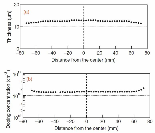
Figure 2: Radial direction distribution of (a) thickness and (b) n-type doping concentration for a 150mm-diameter 4° off 4H-SiC epilayer. Average growth rate 50μm/hour.
Without doping (background n-type ~1013/cm2 carrier density), thickness uniformity of 1.6% σ/mean (6mm edge exclusion) was achieved with 42μm/hour growth rate with fine tuning of the radial gas-flow pattern. The doping uniformity was 2.6% σ/mean with a “peculiar increase in doping concentration near the wafer periphery”. The researchers say that this may be due to “turbulence or temperature variation near the wafer edge, although a very flat distribution of doping concentration is obtained except for the periphery area” (i.e. 11mm edge exclusion).
Silicon carbide SiC SiC Schottky diodes
http://dx.doi.org/10.7567/APEX.7.015502
www.nuflare.co.jp/english/index.html
The author Mike Cooke is a freelance technology journalist who has worked in the semiconductor and advanced technology sectors since 1997.


