


- News
2 January 2014
Thinning nitride LED substrate for increased green emission efficiency
Researchers based in Korea and Egypt have used wafer thinning to increase the efficiency of nitride semiconductor green light-emitting diodes (LEDs) [Wael Z. Tawfik et al, Appl. Phys. Express, vol6, p122103, 2013]. The contributing organizations were Chonnam National University in Korea, Beni-Suef University in Egypt, and Korea Photonics Technology Institute.
The effect of the thinning is to reduce residual compressive stress in the nitride semiconductor structures, which has the knock-on effect of reducing piezoelectric fields in the LED structure. The stress derives from differing thermal expansion coefficients between gallium nitride and sapphire leading to large compressive stress building up as the structure is cooled after the epitaxial crystal growth process.
The effect of the electric fields is to reduce the probability for electrons and holes to recombine into photons. The problem is particularly acute in high-indium-content (more than 20%) indium gallium nitride (InGaN) alloy, as needed for green light emission. While blue InGaN-based LEDs have efficiencies of the order of 50%, the higher-indium-content green LEDs are typically limited to less than 10%.
The LED structures (Figure 1) were grown on 2-inch c-plane sapphire substrates using metal-organic chemical vapor deposition (MOCVD). The substrate thickness was 430μm. The material was formed into 240μm x 600μm LED chips using conventional processes.
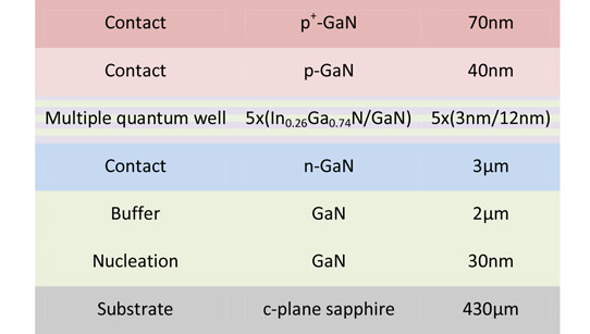
Figure 1: LED epitaxial structure.
The substrate thinning was achieved using back-side lapping and soft polishing. These processes were used to minimize thinning-related damage. After thinning, the chips were singulated in a scribe and break process. Measurements of wafer bowing and residual stress in the n-GaN contact layer showed an increased bow and reduced stress as the wafer was thinned between 200μm and 80μm.
Electroluminescence spectra at 20mA injection current showed an increase in intensity as the substrate was thinned. Also, the peak position shifted from 520.1nm (2.38eV) to 515.7nm (2.40eV) for 200μm- and 80μm-thick substrates, respectively. The researchers explain: “These findings clearly indicate that the mechanical stress introduced by the wafer bowing may change the piezoelectric field in the InGaN/GaN MQW active region and modify the energy band profile. Thus, the blue-shift in peak wavelength and energy are attributed to the increase in effective bandgap due to the decrease in piezoelectric field in InGaN/GaN MQWs.”
The thinning of the substrate also improved internal quantum efficiency (IQE) and light output power, while not degrading the current versus voltage behavior. The light output powers at 20mA increased from 7.8mW with 200μm thickness to 11.5mW with the 80μm-thick substrate. Again, this is credited to the decrease in piezoelectric field enhancing the performance. The forward voltage at 20mA was almost constant at 3.4V across the different thicknesses (200μm, 170μm, 140μm, 110μm, 80μm).
The peak external quantum efficiency (EQE) increased from 16.3% to 24% over the same range of substrate thicknesses (Figure 2). The researchers compare their green LED EQE performance with the best achieved so far on semi-polar free-standing GaN substrates: 20.4% in the (20-21) orientation and 18.9% in the (11-22) orientation. Using semi-polar substrates is another way to reduce piezoelectric effects in GaN-based LEDs. However, such substrates are very expensive.
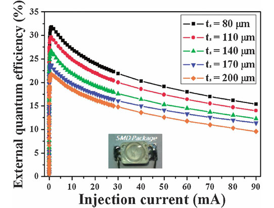
Figure 2: External quantum efficiency (EQE) of green LED as function of injection current with different sapphire substrate thickness. Inset: packaged chip.
The researchers used a room-temperature IQE measurement system from Korean company EtaMax (DOSA-IQE). At less than 10mA injection current the system gave 92% maximum IQE with 80μm substrate thickness. At 20mA, the IQE improved from 58.2% to 68.9% as the substrate was thinned from 200μm to 80μm.
Table 1: Characteristic values of green InGaN/GaN MQW LEDs at an injection current of 20mA with different sapphire substrate thicknesses.
| Sapphire substrate thickness (μm) | 80 | 110 | 140 | 170 | 200 |
| Curvature (/m) | 4.48 | 3.2 | 2.21 | 1.82 | 1.57 |
| Residual stress (GPa) | 0.32 | 0.44 | 0.49 | 0.59 | 0.71 |
| Peak wavelength (nm) | 515.7 | 516.2 | 517.1 | 518.8 | 520.1 |
| Output power (mW) | 11.5 | 10.6 | 9.3 | 8.4 | 7.8 |
| IQE (%) | 68.9 | 64.8 | 62.6 | 60.5 | 58.2 |
| EQE (%) | 24.0 | 22.0 | 19.3 | 17.6 | 16.3 |
| LEE (%) | 34.8 | 33.9 | 30.8 | 29.1 | 28.0 |
| WPE (%) | 17.1 | 15.6 | 13.7 | 12.4 | 11.5 |
By comparing the EQE and IQE, the researchers determined that there was an increase in light extraction efficiency (LEE) with a thinner substrate (Table 1). The improved extraction is attributed to less photon absorption in the sapphire substrate and a higher escape probability from the sapphire edges of the device.
Finally, wall-plug efficiency (WPE) was increased from 11.5% to 17.1% with the same substrate thinning.
http://apex.jsap.jp/link?APEX/6/122103
The author Mike Cooke is a freelance technology journalist who has worked in the semiconductor and advanced technology sectors since 1997.


