


- News
11 February 2014
Enabling high-voltage InGaN LED operation with ceramic substrate
Researchers associated with Taiwan National Central University and Epistar Corp are developing a method to transfer indium gallium nitride (InGaN) light-emitting diodes (LEDs) to ceramic aluminium nitride (AlN) substrates for high-voltage operation [Meng-Lun Tsai and Kun-Yu Lai, Appl. Phys. Express, vol7, p022103, 2014].
The ceramic substrate is more thermally conductive than the sapphire commercially used as a growth substrate for nitride semiconductor heterostructures. The higher thermal conductivity reduces self-heating effects, which negatively impact LED performance.
The high-voltage operation is enabled by connecting 16 electrically isolated sub-devices in series, reducing the injection current and thus delaying the efficiency droop that afflicts nitride semiconductor LEDs at increasing current.
The epitaxial material for the LEDs was grown on c-plane sapphire using metal-organic chemical vapor deposition (MOCVD). The layers consisted of a GaN buffer, n-GaN contact, InGaN/GaN multiple quantum well, p-AlGaN electron-blocking layer, and p-GaN contact. The electroluminescence wavelength was ~450nm (blue).
Fabrication began with deposition of a nickel/silver mirror on the p-contact layer, followed by titanium/aluminium/indium/gold/titanium for flip-bonding to the ceramic AlN substrate. The thermal conductivity of the substrate from Maruwa was 230W/m-K. The sapphire was then detached from the nitride layers using laser lift-off.
The HV-ceramic LEDs are formed by mesa etching down to the ceramic to create 4x4 cell arrays. The n-GaN surface was roughened with a potassium hydroxide wet etch. The purpose of roughening is to enhance light extraction by reducing the total internal reflection at the n-GaN surface due to its large refractive index contrast with air. The sidewalls of the cells were passivated with aluminium oxide. The cells were connected in series with a series of bridges and contacts made with chromium/gold metallization.
Similar devices were produced with transfer to silicon substrates. However, the series connection is difficult to achieve since the substrate is conductive. In view of this, the device consisted of one large cell rather than a 4x4 array to give a low-voltage LED (LV-Si).
Also, HV-sapphire devices were produced in unflipped 4x4 arrays on the original sapphire substrate. Indium tin oxide (ITO) was used as a transparent conducting layer on the p-GaN, followed by aluminium oxide sidewall passivation and the creation of chromium/gold metal bridges and contacts for HV LEDs. An aluminium-based mirror was created on the back-side of the sapphire substrate in an attempt to improve light extraction. The mirror was designed to have 99% reflectance in the blue region of the spectrum.
All the devices measured 45mil x 45mil (1.14mm x 1.14mm). With an injection current density of 76A/cm2, the HV-ceramic device had much better current spreading (Figure 1). The flipped HV-ceramic LED benefited from the lower sheet resistance of the n-GaN window layer, compared with p-GaN. The LV-Si LED suffers from the difficulty of spreading over a wider area. The researchers estimate the sheet resistance of the n-GaN window layer at 15Ω/square, compared with 40Ω/square for the p-GaN window of the HV-sapphire LED.
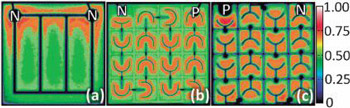 Figure 1: Normalized optical intensities of LEDs driven by current density of 76A/cm2 for (a) LV-Si, (b) HV-sapphire and (c) HV-ceramic. P and N denote p-pad and n-pad, respectively.
The operating voltage of the HV-ceramic LED is higher than that of the HV-sapphire device. This is attributed to the immature nickel/silver/p-GaN mirror contact, compared with the well developed ITO/p-GaN process. The researchers estimate the respective contact resistances at 8mΩ-cm2 and 5mΩ-cm2.
Tsai and Lai comment: “As the preparation of the Ni/Ag alloy is still under development, the operation voltage of the HV-Ceramic device is expected to be reduced once the fabrication parameters are further optimized.”
Output power was measured in an integrating sphere with the LEDs packaged using metal core printed circuit board, but without encapsulation (Figure 2). The measurement stopped when saturation was reached. The HV-ceramic device did not reach saturation before 450A/cm2. “Such a high operation current density of 450A/cm2 is rarely found in the literature,” Tsai and Lai say.
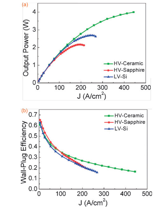
Figure 2: (a) Optical output power vs current density and (b) wall-plug efficiency vs current density for three types of LED.
The saturation of HV-sapphire and LV-Si is mainly attributed to self-heating due to the poorer thermal conductivities of the substrates: 36W/m-K for sapphire, 150W/m-K for Si, and 230W/m-K for ceramic AlN. As the devices heat up, the higher temperature activates defects and increases thermal velocities. Both factors increase non-radiative recombination, reducing efficiency.
The wall-plug efficiencies (WPE) at 210A/cm2 are reduced from the peak values by 70%, 68% and 57%, respectively, for HV-sapphire, LV-Si and HV-ceramic. The WPE of HV-sapphire is slightly higher than the other devices at low currents due to a lower turn-on voltage as a result of the better ITO/p-GaN contact used.
The emission wavelength of the HV-ceramic device is more stable than the other devices. All the LEDs suffer from a blue-shift of about 1.5nm at low injection, due to screening at increased current/carrier densities of the quantum-confined Stark effect of the polarization-dependent electric fields in the structure. At higher currents, self-heating narrows the bandgap, leading to a red-shift.
Between 55A/cm2 and 215A/cm2, the respective red-shifts for HV-sapphire, LV-Si and HV-ceramic are 4.0nm, 1.5nm and 0.5nm. For HV-ceramic, the red-shift at 450A/cm2 is less than 4nm.
LEDs InGaN LEDs GaN Ceramic substrates AlN substrates Epistar MOCVD
http://apex.jsap.jp/link?APEX/7/022103
The author Mike Cooke is a freelance technology journalist who has worked in the semiconductor and advanced technology sectors since 1997.


