


- News
29 December 2014
More absorbent 2D stacks through layer transfer rather than epitaxy
Researchers based in the USA have found that randomly oriented molybdenum disulfide (MoS2) on tungsten disulfide (WS2) has a similar photoluminescence (PL) response to aligned epitaxial structures [Yifei Yu et al, Nano Letters, published online 3 December 2014].
“This work demonstrates that, by stacking multiple two-dimensional (2D) materials in random ways, we can create semiconductor junctions that are as functional as those with perfect alignment,” says Dr Linyou Cao, senior author of the paper and assistant professor of materials science and engineering at North Carolina State University. The other institutions involved in the research were University of North Carolina at Charlotte and Oak Ridge National Laboratory.
Less stringent alignment of semiconductors could lead to an order-of-magnitude lower-cost manufacturing processes, Cao believes.
Yu et al have found that absorption of light in a certain spectral range increased two orders of magnitude over that of single layers of the disulfide materials. Absorption-based photonic devices include photovoltaics/solar cells, solar fuels, photodetectors, optical modulators, and photocatalysts.
Transition-metal dichalcogenides (TMDCs) 2D semiconductors such as MoS2 and WS2 have excited much research interest in the past year. Semiconductor structures usually need to be precisely aligned with matched lattice structures for efficient operation. “But we found that the crystalline structure doesn’t matter if you use atomically thin, 2D materials,” Cao comments. “We used molybdenum sulfide and tungsten sulfide for this experiment, but this is a fundamental discovery that we think applies to any 2D semiconductor material. That means you can use any combination of two or more semiconductor materials, and you can stack them randomly but still get efficient charge transfer between the materials.”
The epitaxial MoS2 and WS2 heterostructure was produced through chemical vapor deposition (CVD) in a tube furnace with sulfur and molybdenum and tungsten oxide precursors (MO3, WO3). Epitaxial structures were grown at 950°C with a flow of argon.
The synthesized MoS2 and WS2 monolayer 2D crystals formed as large (~25μm) or small triangles (~8μm), respectively. These formed concentric heterostructures (Figure 1). The lattice constants of the two materials were almost identical.
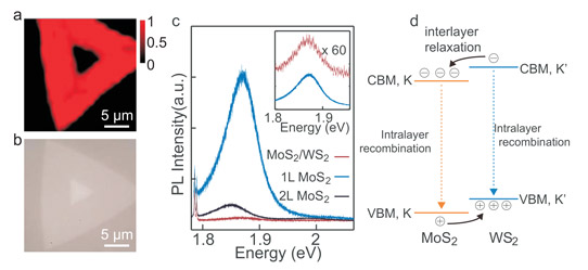
Figure 1: (a) PL mapping of typical epitaxial MoS2/WS2 heterostructure. (b) Optical image of heterostructure mapped in (a). (c) PL spectra collected from monolayer (1L) MoS2 area (red curve) and MoS2/WS2 heterostructure area (blue curve). PL from MoS2 bilayer (2L) is also given (black curve). Inset: comparison of PL from MoS2 and MoS2/WS2 areas, where PL from MoS2/WS2 area is scaled by factor of 60. (d) Schematic illustration of bandstructure alignment of heterostructure. K-point of MoS2 coincides with the K’-point of WS2. Interlayer relaxations and intralayer recombination are also shown.
Photoluminescence from regions of MoS2 away from the heterostructure gave a peak at 1.87eV, consistent with other measurements made on MoS2 monolayers (Figure 1). In the region of the heterostructure, the peak is reduced by about two orders of magnitude (factor of 100). A bilayer of MoS2 also showed a reduced intensity peak, but only about an order of magnitude.
The researchers point out that they do not see a 1.4eV peak found by another group in WS2/MoS2 heterostructures. The team suggests that differences in WS2 growth precursors or the different substrates used might explain the different characteristics. The tungsten precursor used by Yu et al was WO3, while the other group used a combination of tungsten and tellurium. The respective substrates were sapphire and silicon dioxide/silicon. Yu et al attribute the PL suppression to interlayer exciton relaxation.
Non-epitaxial structures were fabricated by manually combining separate WS2 and MoS2 layers. The separate layers were grown at lower temperatures – 750°C for MoS2 and 900°C for WS2. For the WS2 process, 5% hydrogen was added to the argon carrier.
The MoS2 layer was delaminated from the growth substrate through a surface-energy-assisted transfer process involving polystyrene and water. The polystyrene/MoS2 was handled with tweezers and transferred onto WS2. The polystyrene was removed with toluene. Annealing was carried out on some samples at 200-250°C for 10-30 minutes in argon.
The MoS2 was around 5μm, stacked on ~50μm WS2. The annealed non-epitaxial structures showed similar two-order of magnitude decreases in PL intensity in overlap regions. Without annealing, the decrease is less significant. The researchers comment: “The low-temperature annealing process may remove the residue of solvent and water molecules left between the two monolayers during the transfer process, which may subsequently facilitate the interlayer exciton relaxation.”
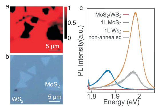
Figure 2: (a) PL mapping of typical non-epitaxial MoS2/WS2 heterostructures. (b) Optical image of heterostructure mapped in (a) with multiple MoS2 monolayers (small triangles) randomly distributed on top of big WS2 monolayer. (c) Spectra PL collected from non-epitaxial MoS2/WS2 heterostructure (red curve), MoS2 monolayer (1L) (blue curve), and WS2 monolayer (1L) (brown curve). PL from unannealed non-epitaxial MoS2/WS2 heterostructure is also given (grey curve).
The researchers also say that the PL response is independent of the crystal orientation of the stacked layers. They add: “The independence of the efficient interlayer exciton relaxation in MoS2/WS2 heterostructures on the epitaxy and orientation of the stacking suggests a strong electron-phonon coupling in 2D materials. The electron-photon coupling could be so strong that it is able to efficiently compensate for any momentum mismatch of the charge transfer between the monolayers.”
Other groups have measured much less decrease of the PL – around a factor of three. The team suggests that this could be due to the different layer transfer processes used that can cause damage or leave organic residues. Also, the substrates may again be to blame.
http://pubs.acs.org/doi/abs/10.1021/nl5038177
The author Mike Cooke is a freelance technology journalist who has worked in the semiconductor and advanced technology sectors since 1997.


