


- News
12 August 2014
Increasing light output from InGaN LEDs on silicon wafer
China’s Nanjing University of Posts and Telecommunications has improved the performance of indium gallium nitride (InGaN) light-emitting diodes (LEDs) on silicon (Si) substrate by removing the substrate from the region under the device [Zheng Shi et al, Appl. Phys. Express, vol7, p082102, 2014].
InGaN LEDs produce light with relatively short wavelengths that are strongly absorbed by silicon since the photon energies exceed the latter material’s bandgap. Removing the silicon substrate material from under the LED – giving a free-standing membrane of nitride semiconductor material – increases the ability of the light to escape the device.
The researchers believe that substrate removal could also allow wavelength tuning and integration with cooling systems to reduce thermal degradation at high-power operation.
The epitaxial nitride semiconductor structure (Figure 1) used thick buffer layers to bridge the lattice and thermal expansion mismatches between GaN and Si.
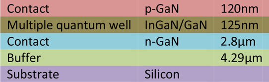
Figure 1: Epitaxial structure.
Fabrication (Figure 2b) began with spin coating photoresist on the epitaxial structure (a), followed by patterned reactive ion etch down to the n-GaN layer to form a mesa (b). Then, the n- and p-contact regions were patterned and nickel/gold semi-transparent metal ohmic contacts were deposited and annealed (c).
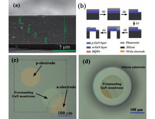
Figure 2: (a) Cross-sectional SEM image of LED; (b) schematic of fabrication of free-standing membrane LED; (c) optical microscopy image of free-standing LED; (d) optical microscopy image of silicon substrate.
More photoresist was applied to the top surface before deep reactive ion etch was used to remove the silicon substrate from the under-side of the LED, using the buffer as an etch-stop (d). The free-standing membrane device was finished with the removal of residual photoresist (e).
The LED chip area was 400μmx400μm, with the p-electrode diameter 100μm and n-electrode quarter circle radius 150μm. The designed hole diameter in the silicon was 200μm and the membrane diameter was 142μm. The researchers were concerned that a too wide free-standing region would not be able to sustain residual stresses in the structure. The sidewall angle of the hole was 81.5°.
Photoluminescence increased with the removal of the silicon substrate from under the LED region. Spectral analysis also showed a blue-shift in the emission peak. Multiple reflections gave interference fringes in the spectrum.
The researchers comment on the current-voltage (I–V) performance that “considerable improvement of the I–V characteristics for the free-standing membrane LED may be attributed to the reduction of the spreading resistance and the increase in the conductivity”. The removal of silicon from underneath the device reduced the turn-on voltage by about 1V.
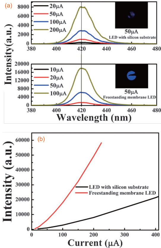
Figure 3: (a) Room-temperature electroluminescence spectra of LEDs under different continuous current injections. Inset: top view of fabricated LEDs under 50μA current; (b) peak emission intensity of fabricated LEDs as function of injection current.
The membrane device had a strong electroluminescence at 420nm (Figure 3). The researchers say that the slope of increased emission with current injection was about six times larger for the free-standing membrane structure.
LEDs InGaN InGaN LEDs Silicon wafer
http://dx.doi.org/10.7567/APEX.7.082102
The author Mike Cooke is a freelance technology journalist who has worked in the semiconductor and advanced technology sectors since 1997.


