


- News
21 August 2014
High-electron-mobility light-emitting devices for optoelectronics
Hong Kong University of Science and Technology (HKUST) has developed 365nm ultraviolet (UV) light-emitting diodes (LEDs) on undoped high-electron-mobility (HEM) aluminium gallium nitride (AlGaN) structures [Baikui Li et al, Appl. Phys. Lett., vol105, p032105, 2014].
UV LEDs are normally produced using variously doped layers of indium gallium nitride or aluminium gallium nitride. By contrast, GaN-based transistors use undoped AlGaN and GaN layers to create a two-dimensional electron gas (2DEG) channel through contrast in the polarization of the two materials. GaN-based transistors are being developed for radio frequency high-power amplification wireless transmission and switched power supply devices.
The HKUST light emitters used the AlGaN/GaN structure of HEM transistors (HEMTs) and Schottky diode contacts. The researchers see potential for compact optoelectronic systems, such as on-chip lighting control and opto-couplers for electrical power conversion. Another possible use would be in microdisplays where the 2DEG channel would provide the back electrode and a Schottky contact would define the pixel.
The researchers produced both LEDs and light-emitting transistors (HEM-LETs) on heterostructures consisting of a 21nm Al0.25Ga0.75N barrier on 3.8μm GaN buffer. The substrate for the metal-organic chemical vapor deposition (MOCVD) was 4-inch p-type silicon (111). The heterostructure contained a 2DEG channel of density 1013/cm2 and mobility 2080cm2/V-s.
Ohmic contacts consisted of annealed titanium/aluminium/nickel/gold. Atomic layer deposition (ALD) equipment was used to remove native oxide from the surface, nitridize the heterostructure surface, and deposit 4nm aluminium nitride (AlN). Plasma-enhanced chemical vapor deposition (PECVD) added a 50nm silicon nitride (SiNx) layer. The AlN/SiNx layers provided passivation and surface protection.
The Schottky contact was fabricated by selectively removing the passivation/protection with a combination of plasma and wet etch. The semi-transparent 5nm/6nm nickel/gold Schottky contact was deposited using electron-beam evaporation.
The transistor had an ohmic source and semi-transparent Schottky drain. The gate stack included 15nm/8nm silicon nitride/aluminium oxide (AlO) insulation and 20nm/200nm nickel/gold electrode. The transistor was annealed at 400°C for 10 minutes in nitrogen atmosphere.
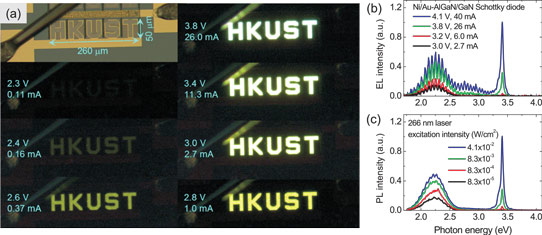
Figure 1: (a) Visible electroluminescence (EL) of Ni/Au-AlGaN/GaN Schottky diodes under different forward biases from 2.3V to 3.8V. (b) EL spectra of diode under different bias/current conditions. (c) Photoluminescence spectra of heterostructure excited by 266nm laser at various excitation powers.
The Schottky diode emitted electroluminescence when biased above 2.2V. The spectrum contained yellow, blue and UV emissions (Figure 1). The UV component consisted of a narrow peak at around the GaN bandgap of 3.4eV. The yellow and blue emissions were broad, associated with transitions from the conduction band or shallow donor level to deep acceptor levels. All the emissions were attributed to the GaN buffer and not the AlGaN barrier layer. The balance between the UV and yellow/blue components shifted to the UV as the injection current increased. Similar spectra were obtained with photoluminescence.
The current-voltage behavior of the diode shows a current threshold at 1.1V and a further threshold at ~2V, associated presumably with the onset of electroluminescence.
The onset of electroluminescence at ~1.4V below the 3.4V expected from the bandgap energy indicates “an abnormal anti-Stokes light emission process”. Anti-Stokes emission refers to an energy boost coming from thermal phonons (lattice vibrations). The researchers believe the hole injection results from de-pinning of the Fermi level of the Schottky metal contact under forward bias.
The researchers explain: “Under a forward bias, electrons are injected from the 2DEG and accelerated by the electric field in the AlGaN barrier. Then, the electrons become ‘hot’ when arriving at the Ni-AlGaN interface. These hot electrons will impact and ionize the upper surface-band states. As electrons in the upper surface-band are ionized, the metal Fermi level is de-pinned simultaneously from its original position, subsequently moving downward and getting re-pinned at the lower surface-band. Then, both the energy barrier height and effective barrier thickness become considerably smaller for hole injection via tunneling from the metal Fermi level into the valence band of AlGaN.”
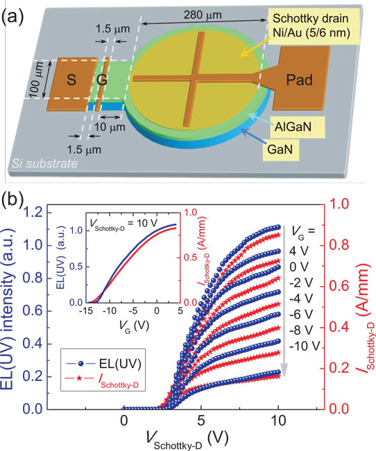
Figure 2: (a) Schematic device structure of AlGaN/GaN HEM-LET. (b) Current (I) versus voltage (V) for Schottky drain (D) (red line) and EL(UV)-intensity (blue line) characteristics at various gate (G) biases. Inset provides EL(UV)-intensity and drain current versus gate voltage at 10V drain.
The researchers estimate the room-temperature light output power from a 10-3cm2 Schottky light-emitting diode area at 11.2μW at 4V bias, corresponding to 71mA current. The HEM-LET has a similar 2V threshold for electroluminescence from the drain electrode (Figure 2). HEMTs produced on the same heterostructure had an off-state leakage of 10-6mA/mm and an on/off current ratio of 108.
UV LEDs AlGaN HEMTs Schottky diodes MOCVD ALD PECVD
http://dx.doi.org/10.1063/1.4890238
The author Mike Cooke is a freelance technology journalist who has worked in the semiconductor and advanced technology sectors since 1997.


