


- News
21 April 2014
Growing InGaAs MOSCAPs directly on (100) silicon substrates
Researchers in Taiwan have produced indium gallium arsenide (InGaAs) metal-oxide-semiconductor capacitors (MOSCAPs) with low interface trap densities directly on silicon [Yueh-Chin Lin etal, Appl. Phys. Express, vol7, p041202, 2014]. InGaAs is a high-mobility semiconductor that should improve transistor characteristics for high-frequency applications.
MOSCAPs with low trap densities are an important step towards producing high-performance MOS field-effect transistors (MOSFETs). In effect, MOSCAPs are MOSFETs without source/drain contacts. Reducing the trap density at the dielectric/semiconductor interface is vital for good electrostatic control by the gate in MOSFETs.
Often, InGaAs heterostructures are grown first on indium phosphide (InP) substrates and then transferred to silicon by wafer bonding techniques. The team from National Chiao-Tung University and Taiwan Semiconductor Manufacturing Company (TSMC) grew their InGaAs heterostructure (Figure 1) on 300mm (100) silicon (Si) substrates directly by metal-organic chemical vapor deposition (MOCVD).
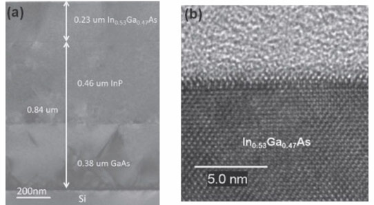
Figure 1: Transmission electron micrographs of InGaAs/Si heterostructure (a) and high-resolution close-up of InGaAs channel region (b).
The first buffer layer of strained GaAs was designed to metamorphically bridge the lattice mismatch between silicon and the InP buffer and lattice-matched In0.53Ga0.47As ‘channel’. The GaAs/InP metamorphic combination was 840nm thick: “the thinnest buffer for the growth of In0.53Ga0.47As on a Si substrate reported to date,” according to the researchers.
Analysis of the sample suggested that the dislocations were predominantly trapped in the GaAs layer. The dislocations in the In0.53Ga0.47As layer were estimated at 2−3x10⁹/cm2, according to x-ray diffraction (XRD) measurements. Atomic force microscopy (AFM) of the In0.53Ga0.47As surface gave a root-mean square roughness of 1.94nm averaged over a 5μmx5μm field. This in the range given by previous In0.53Ga0.47As growth on Si with thicker GaAs/InP buffers.
Room-temperature Hall mobility measurements gave values in excess of 5000cm2/V-s, comparable to InGaAs grown on InP substrates.
The metal-oxide-semiconductor capacitors (MOSCAPs) were fabricated by surface treatment, aluminium oxide and gate metal deposition, and Ohmic contact formation. The 8nm-thick oxide was applied using atomic layer deposition (ALD) at 300°C, followed by a 10-minute anneal process in nitrogen gas. The gate metal layers consisted of nickel and gold. The Ohmic contact was constructed by etching the oxide with hydrofluoric acid, revealing the InGaAs surface, and then depositing and annealing gold/germanium/nickel/gold metal contacts.
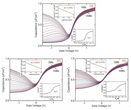
Figure 2: Capacitance-voltage curves for samples with silicon-doped InGaAs layers with oxide annealed at 400°C: (a) 8.0x10¹⁶/cm3, (b) 1.7x10¹⁷/cm3, (c) 6.2x10¹⁷/cm3.
According to capacitance versus voltage measurements (Figure 2), the aluminium oxide anneal process gave fewer interface traps at 400°C (5.44−5.87x10¹¹/cm2-eV), compared with a similar sample annealed at 500°C (1.45−1.62x10¹²/cm2-eV). With 400°C annealing, the frequency dispersion was small and the hysteresis “excellent” (Table 1).
Table 1: Parameters of InGaAs MOSCAPs with Al2O3 annealing at 400°C.
| Doping | Interface trap density | Frequency dispersion | Hysteresis |
| 8.0x10¹⁶/cm3 | 5.80x10¹¹/cm2-eV | 2.74%/decade | 76mV |
| 1.7x10¹⁷/cm3 | 5.87x10¹¹/cm2-eV | 2.52%/decade | 65mV |
| 6.2x10¹⁷/cm3 | 5.44x10¹¹/cm2-eV | 2.37%/decade | 84mV |
The researchers conclude the performance of their Al2O3/InGaAs/Si MOSCAPs was comparable to Al2O3/InGaAs on lattice-matched InP. “The results demonstrate the potential of integrating an InGaAs-based material on a 12-inch Si substrate by MOCVD for future high-performance low-power logic device applications and mainstream manufacturing.”
InGaAs Silicon substrates MOSFETs InP substrates MOCVD ALD
http://iopscience.iop.org/1882-0786/7/4/041202/article
The author Mike Cooke is a freelance technology journalist who has worked in the semiconductor and advanced technology sectors since 1997.


