


- News
18 April 2014
Top-down InGaAs nanowire fabrication enabled by novel etch processing
Massachusetts Institute of Technology (MIT) researchers Xin Zhao and Jesús A. del Alamo have developed a ‘novel’ inductively coupled plasma reactive-ion etch (ICP-RIE) process that can produce sub-20nm vertical indium gallium arsenide (InGaAs) nanowires (NWs) with aspect ratios exceeding 10 [IEEE Electron Device Letters, published online 4 April 2014]. The technique also uses an extra ‘digital etch’ to mitigate surface damage of the nanowires caused by the aggressive ICP-RIE.
Vertical nanowire transistors could be a means to pack more devices into three-dimensional (3D) integrated circuits. Using a high-mobility semiconductor nanowire such as InGaAs should lead to higher performance. The technique often used by researchers to create such nanowires involves a gold seed placed on the surface of the substrate that subsequently drags out a nanowire in a ‘bottom-up’ growth process.
However, such bottom-up growth processes are difficult to control in manufacture and some researchers would like to develop a more traditional ‘top-down’ fabrication. Also, the use of gold would be forbidden in devices that included silicon CMOS components alongside the high-mobility transistors.
The MIT etch process was performed on In0.53Ga0.47As heterostructure material grown on indium phosphide (InP) substrates using metal-organic chemical vapor deposition (MOCVD). The InGaAs heterostructure consisted of an 80nm undoped channel sandwiched between n+ silicon-doped contacts.
The vertical nanowire patterning was defined by electron-beam lithography on hydrogen silsesquioxane (HSQ) resist to give a mask for the RIE. Zhao and del Alamo used a SAMCO RIE-200iP ICP system with a heated chuck and backside helium cooling.
The plasma chemistry consisted of boron trichloride, silicon tetrachloride and argon (BCl3/SiCl4/Ar). The SiCl4 was found to improve the verticality of the sidewalls. The BCl3/Ar balance affects surface roughness and selectivity against the HSQ mask.
Zhao and del Alamo sought to optimize substrate temperature (250°C), gas flows (7sccm/0.55sccm/7sccm for BCl3, SiCl4 and Ar, respectively), chamber pressure (0.2Pa), and ICP and RF platen powers (20W/160W). These conditions etch at a rate of 1.8nm/second with an 8:1 selectivity against the HSQ mask. The substrate bias voltage was 280V.
The optimized process was used to create vertical nanowires of 15nm and 28nm diameters and 240nm heights. Zhao and del Alamo admit that further process development is needed to address “a slight footing behavior towards the bottom of the nanowire and some degree of trenching” (Figure 1).
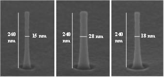 Figure 1: (a) 15nm-diameter InGaAs NW defined by optimized RIE technique with an aspect ratio greater than 15. (b) 28nm-diameter InGaAs NW fabricated by RIE. (c) Same NW as in (b) after 5 subsequent cycles of digital etch.
The digital etch process consisted of a two-step cycle: a self-limiting low-power O2 plasma oxidation and a diluted sulfuric acid (H2SO4) rinse to remove the oxide. Several cycles of the process were carried out to repair RIE damage from the vertical sidewalls of the nanowires. One cycle of the digital etch process resulted in a ~2nm reduction in nanowire diameter.
Zhao and del Alamo fabricated gate-all-around nanowire transistors with 4.5nm atomic layer deposition (ALD) aluminium oxide gate dielectric (with an equivalent oxide thickness of 2.2nm). The channel was nominally 80nm – the thickness of the undoped channel layer in the InGaAs heterostructure.
The researchers compared 30nm-diameter nanowire transistors with and without 10-cycle digital etch (Figure 2). The RIE for the digital etch transistors created 50nm-diameter wires that were reduced to 30nm diameter by the digital etch. Scanning electron microscopy (SEM) was used to confirm that the wires for the two types of device were of identical diameter within experimental uncertainties.
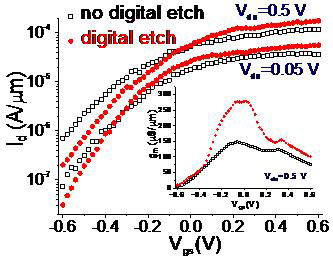 Figure 2: Impact of digital etch on subthreshold and transconductance (inset) characteristics of 30nm-diameter gate-all-around InGaAs NW-MOSFETs.
The effect of digital etch was to reduce the subthreshold swing from 190mV/dec to 150mV/dec at 0.05V drain bias. Also, the transconductance with 0.5V drain bias increased from 155μS/μm to 280μS/μm with digital etch. The on-current at 1V gate overdrive and 0.5V drain bias was 205μA/μm with digital etch, but only 130μA/μm without. The on-resistance for both devices was 760Ω-μm.
The improvements are attributed to the reduction in sidewall damage provided by the digital etch.
Zhao and del Alamo comment that their top-down devices match the short-channel and transconductance performance of transistors made with bottom-up techniques. However, planar III-V MOSFETs have demonstrated better transconductance. The researchers blame the high equivalent oxide thickness of their dielectric and the high series resistance of the contacts.
Plasma etch InGaAs nanowire InP substrates MOCVD Samco
http://ieeexplore.ieee.org/xpl/articleDetails.jsp?arnumber=6783795
The author Mike Cooke is a freelance technology journalist who has worked in the semiconductor and advanced technology sectors since 1997.


