


- News
6 September 2013
ITO cladding to reduce thermal damage in blue/green III-nitride lasers
Researchers from the universities of California Santa Barbara (UCSB) and of New Mexico (UNM) have demonstrated semipolar nitride semiconductor blue and green laser diodes (LDs) with part of the upper cladding replaced by indium tin oxide (ITO) [Matthew T. Hardy et al, Appl. Phys. Lett., vol103, p081103, 2013].
Cladding layers use a difference in refractive index to confine light in LD waveguide structures. These layers are also doped to provide injection of electrons and holes into the active light emitting region.
One problem for nitride semiconductor structures aimed at blue and green emission is that the active and waveguide regions contain indium gallium nitride (InGaN) for which the optimum growth temperature is lower than that required for cladding layers of gallium nitride (GaN) or aluminium gallium nitride (AlGaN). The higher temperature needed for the upper cladding layer can damage the underlying InGaN layers.
Replacement of part of the upper cladding with ITO reduces the amount of growth time at elevated temperatures, reducing thermal damage.
The UCSB/UNM team sees its new process as more closely resembling that of light emitting diodes (LEDs) than the usual process for LDs that involves AlGaN cladding. One difference is a striking reduction in growth time from ~7 hours for AlGaN-clad structures to ~3 hours for the nitride epitaxy for the ITO-clad LDs.
Mistubishi provided the freestanding GaN substrates with semipolar crystal orientation (20-21). Semipolar light-emitting devices benefit from reduced electric fields that arise from the strongly ionic nature of the chemical bonds in nitride semiconductors. Reduced fields improve the recombination rates of electrons and holes into photons in the active region.
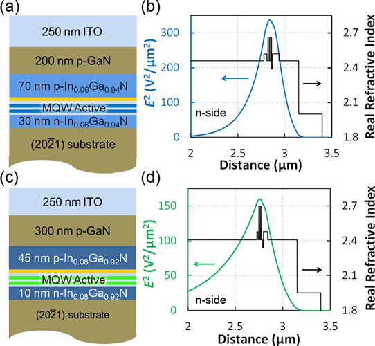
Figure 1: Blue ITO-clad LD (a) schematic epitaxial structure and (b) square of the electric field and refractive index as function of distance in the growth direction (transverse mode profile). Green ITO-clad LD (c) schematic epitaxial structure and (d) transverse mode profile.
The nitride semiconductor epitaxial structures (Figure 1) were grown using horizontal-flow atmospheric-pressure metal-organic chemical vapor deposition. The thicknesses of the top p-GaN cladding layers were chosen as a compromise between maximizing optical confinement and minimizing the GaN thickness, as determined by simulations.
The growth temperatures of the p-GaN cladding were 950°C for the blue laser and 840°C for the green. The lower temperature for the green LD was to avoid thermal damage of the more delicate quantum wells with higher indium content that are used for green emission. Also, triethyl-gallium rather than trimethyl-gallium was used for the green LD p-GaN growth to avoid carbon incorporation due to the lower growth temperature. Carbon incorporation can reduce crystal quality and increases resistivity.
The multiple quantum well (MQW) active light-emitting regions were 3-period InGaN/GaN structures. The blue LD well/barrier thicknesses were 4.5nm/10nm. The respective thicknesses for the green device were 2.7nm/10nm. Both LDs also included an electron blocking layer consisting of 10nm of aluminium gallium nitride (Al0.2Ga0.8N) above the MQW. The InGaN waveguide thicknesses were determined from the design/simulation process.
The epitaxial material was formed into ridge waveguide LDs with etched facets using a self-aligned via process. The ridges were aligned with the in-plane projection of the c-direction ([-1014]). The reactive ion etch (RIE) was performed using a chlorine-based process that terminated about 100nm above the MQW layer. A 250nm layer of silicon dioxide was deposited and self-aligned vias opened using a lift-off process based on the ridge waveguide photoresist mask.
The 250nm ITO deposition and anneal was performed off-site at MES AFTY Corporation, Tokyo, Japan. MES AFTY used its own electron cyclotron resonance (ECR) plasma deposition system for the ITO growth, along with Chemitronics Co., Ltd.’s Ohmic Alloy system for the anneal.
The off-site ITO process meant that standard lift-off techniques were not possible, so the researchers used a methane/hydrogen/argon RIE process to isolate the devices and to remove ITO from the facets. This etch process was highly selective for ITO with respect to the silicon dioxide and GaN.
The devices were completed with the addition of titanium/gold p-contacts and aluminium/gold n-contacts. No coatings were applied to the facets.
Pulsed operation of a 7.5x1800μm blue LD found a threshold current of 6.2kA/cm2 at 8.9V bias. At 1.2x the threshold current, the spectral peak was centered at 471nm. Similarly, a 2x1500μm green LD under pulsed operation had a threshold current of 40kA/cm2 at 14V. The emissions were around 518nm at 1.3x threshold (Figure 2). The high operating voltages are blamed tentatively on unoptimized contacts and doping profile.
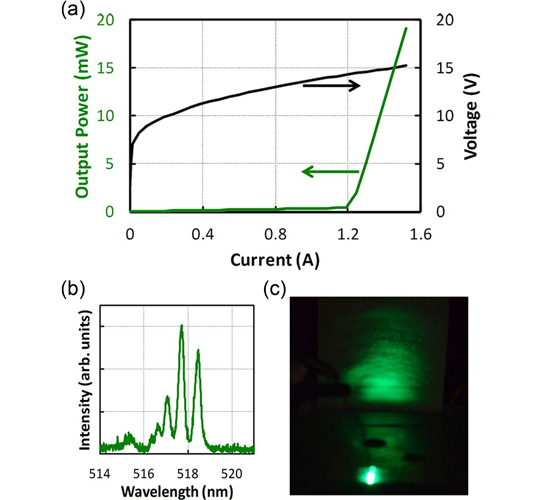
Figure 2: (a) Light–current–voltage characteristics, (b) multi-mode lasing spectra around 518nm, and (c) far-field image for 2x1500μm uncoated ITO-clad green LD under pulsed operation.
The researchers comment that the blue LD’s threshold current is “competitive with other uncoated LDs in this wavelength regime and better than our standard GaN-clad (20-21) blue LDs with the same active region and a similar device structure and processing technology.”
Another improvement of the ITO-clad LDs is a decrease in differential resistance to 2Ω for the blue device and 3Ω for the green. UCSB’s conventional LDs with p-GaN cladding have typical differential resistances in the range 5-8Ω. The researchers attribute the lower differential resistance to reduced p-GaN thickness and the much lower bulk resistivity of ITO.
The researchers would like to add an n-cladding layer with greater refractive index contrast to increase the optical confinement factor and to enhance device performance.
http://link.aip.org/link/doi/10.1063/1.4819171
The author Mike Cooke is a freelance technology journalist who has worked in the semiconductor and advanced technology sectors since 1997.
