


- News
4 October 2013
Exploring nanopyramid approach to longer-wavelength nitride LEDs
Researchers in Taiwan have used nanopyramid nitride semiconductor structures to explore long-wavelength green, olivine and amber light-emitting diode (LED) structures [Shih-Pang Chang, Optics Express, Vol. 21, p23030, 2013].
The team was variously based at National Chiao Tung University and Academia Sinica’s Research Center for Applied Sciences. The researchers also used technical expertise from Epistar Corp, LuxtalTek Corp and Industrial Technology Research Institute (ITRI), all similarly based in Taiwan.
The device performances compared favorably with LEDs produced on c-plane sapphire. It is thought that producing the light-emitting structures on the semi-polar facets of hexagonal gallium nitride (GaN) nanopyramids reduces the spontaneous and strain-dependent (piezo-) electric fields that arise in indium gallium nitride (InGaN) quantum wells. These fields in polar c-plane devices keep the electrons and holes from recombining into photons, reducing efficiency.
Although semi-polar and even non-polar substrates can be produced, they are not readily available.
The fabrication process (Figure 1) began with an n-type gallium nitride (n-GaN) template on sapphire. First, nanocolumns were formed in a patterned etch. The column sidewalls were coated with spin-on glass (SiO2). The GaN semiconductor nanopyramids, with additional indium gallium nitride (InGaN)/gallium nitride (2nm/8nm) multiple quantum wells (MQWs) and a p-GaN top contact, were grown by metal-organic chemical vapor deposition (MOCVD) on the tops of the nanocolumns. The spin-on glass coating was aimed at blocking re-growth of nitride semiconductor on the sidewalls of the columns.
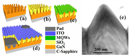
Figure 1: Fabrication steps of nanopyramid LED. (a) Patterned top-down etch of nanopillars. (b) Nanopillar sidewall coated with oxide. (c) Nanopyramids grown on top of nanopillars, followed by MQW growth. (d) Top surface indium tin oxide (ITO) deposition and metal pad fabrication. (e) HRTEM cross-section image taken from nanopillar sample right after MQW growth.
Further processing included applying indium tin oxide (ITO) transparent top contact and mesa etching to reach the n-GaN contact layer to create 300μm x 300μm LEDs. Three different emission types were produced by varying the indium content of the InGaN wells. The peak wavelengths at 100mA were 500nm (green/G), 550nm (olivine/O) and 600nm (amber/A).
A number of techniques were used to assess the quality of the materials. High-resolution transmission electron micrography (Figure 1e) showed darker regions in the InGaN towards the bottom and apex of the nanopyramids. The researchers suggest that this could be due to non-uniform indium content and coalescent defects.
Cathodoluminescence microscopy on the G-LED material showed variations in emission wavelengths with position in the nanopyramid, attributed to variations in indium content of the InGaN wells. An energy-dispersive spectrometer (EDS) x-ray system measured a variation in indium content from the base to apex region of 15% to 30%. There was no significant variation in well thickness.
Temperature dependent photoluminescence measurements between 20K and 300K were used to give internal quantum efficiency assessments: 30%, 25% and 21%, for the G-, O- and A-LEDs, respectively. The values are high compared with a typical value of 12% for c-plane MQWs emitting at 570nm. The decline in IQE for higher-indium-content quantum wells is attributed to a “larger internal polarization field, which results in larger electron-hole wavefunction separation”.
The behavior of the photoluminescence lifetime temperature dependence is also different from traditional c-plane MQWs. In particular, there is no red-blue-red shift (‘S-curve’) behavior. The researchers comment: “The absence of S-curve implies a significant reduction of localized potentials for MQWs grown on the nanopyramid facets. This could be due to the better strain relaxation provided by the nanostructure and/or the growth property of the pyramid semi-polar facets.”
Under electrical injection (Figure 2), the turn-on voltage of the LEDs was around 3V. At higher currents the voltage increases significantly to 6V at 200mA, higher than usual for c-plane LEDs. The researchers believe that the diodes had a high series resistance due to an imperfect contact between the ITO layer and the corrugated surface of the nanopyramid array.
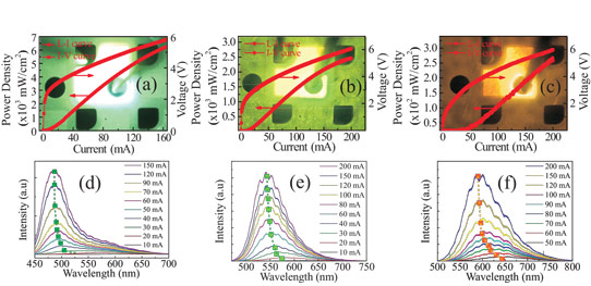
Figure 2: (a)-(c) Optical microscope images of G-, O- and A-LED under electrical injection, showing green, olivine and amber colors. (d)-(f) Electroluminescence spectra versus injection current, showing blue-shift of peak emission as current increases due to screening of polarization field.
Light output from the devices is slow to turn on, particularly in the longer-wavelength A-LED, which does not operate before 40mA. This problem is attributed to current leakage effects. The higher amount of defects in the base and apex regions is blamed.
With increased current the spectrum peak of light output undergoes a blue-shift of 13nm, 25nm and 50nm, for the G-, O- and A-LEDs, respectively. “These blue-shift values are, nevertheless, still relatively small compared with that in a c-plane MQW,” the researchers point out.
The indium composition gradient leads to rather broad emission spectra with full-width at half-maximum values, respectively, for the G-, O- and A-LEDs of 60nm, 80nm and 110nm. The researchers see possible applications for LEDs with even broader spectra as phosphor-free white-light LEDs.
http://dx.doi.org/10.1364/OE.21.023030
The author Mike Cooke is a freelance technology journalist who has worked in the semiconductor and advanced technology sectors since 1997.


