


- News
15 October 2013
Improving gate swing and avoiding current collapse in GaN MIS-HEMTs
Hong Kong University of Science and Technology (HKUST) has developed a 600V gallium nitride on silicon (GaN/Si) normally-off metal-insulator-semiconductor high-electron-mobility transistor (MIS-HEMT) with large gate swing and low current collapse [Zhikai Tang et al, IEEE Electron Device Letters, published online 17 September 2013].
Normally-off ‘enhancement-mode’ transistors are needed for power switching applications at high voltage to provide fail-safe operation. A further advantage of normally-off operation is low power consumption.
Conventional GaN-based HEMTs tend to operate in depletion mode where the transistor is ‘ON’ at 0V gate potential. The HKUST team raised the threshold voltage of their devices by using fluorine plasma implantation and using silicon nitride as a gate insulator.
The MIS-HEMTs also featured a passivation layer that combined aluminium nitride (AlN) and silicon nitride (SiN) to avoid current collapse effects from charge trapping that often occur in GaN-based HEMTs in high-speed pulsed operation.
The epitaxial aluminium gallium nitride (AlGaN) structure was grown on 4-inch p-type (111) silicon. Processes that grow GaN-based HEMTs on silicon offer potential cost-reductions for manufacturing. The buffer/transition GaN layer was 4μm, on which was added a 1nm AlN spacer, 18nm Al0.25Ga0.75N barrier, and 2nm GaN cap.
Transistor fabrication began with deposition of ohmic source–drain contacts of thermally annealed titanium/aluminium/nickel/gold. Passivation layers of 4nm AlN then 50nm SiN were added by plasma-enhanced atomic layer deposition (PE-ALD) then plasma-enhanced chemical vapour deposition (PECVD), respectively. Device isolation was achieved using fluorine ion implantation.
Gate formation consisted of making an opening in the passivation layers using a low-power dry etch, treating the gate region with carbon tetrafluoride plasma implantation to shift the threshold voltage to enhancement mode, removal of photoresist, ex-situ plasma cleaning in a plasma-enhance atomic layer deposition system to remove surface gallium–oxygen bonds, applying another 17nm of PECVD SiN as gate insulator, and formation of the nickel/gold gate electrode with 1μm footprint and 0.5μm overhang.
Further dimensions of the tested devices were 1μm gate–source spacing, 10μm gate width and 15μm gate–drain spacing. The resulting MIS-HEMTs were found to have a threshold voltage of +3.6V, giving enhancement-mode, normally-off behavior. Comparison HEMT devices with Schottky gate had a lower threshold of +1.2V. The difference is primarily attributed to “reduced gate-to-channel capacitance by the insertion of the SiNx gate dielectric” in the MIS-HEMT.
The on/off current ratio was 4x10⁹ with a maximum drain current of 430mA/mm. The suppression of gate leakage current enabled by the SiN insulation allowed the device to demonstrate a 14V gate swing. Traditional Schottky-gate GaN HEMTs tend to have the gate swing restricted to less than 3V. The on-resistance for the MIS-HEMT was a ‘low’ 9.8Ω-mm. The specific on-resistance was estimated at 2.1mΩ-cm2.
Off-state breakdown with a drain current of 1μA/mm occurred at a drain bias of 604V with the gate, source and substrate grounded (0V). Up to 450V, the main leakage comes from the source. At higher biases, gate and vertical substrate leakage increase and become comparable with the source current at 600V. The researchers compared their device with other published results (Figure 1).
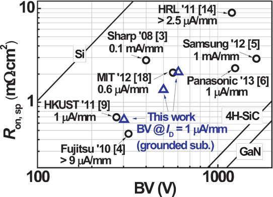
Figure 1: Specific on-resistance (RON) versus breakdown voltage (BV) of some state-of-the-art GaN-based normally-OFF power devices. OFF-state leakage criteria in defining the OFF-state breakdown voltage in different reports are highlighted.
The researchers stress the need for a low off-state current of less than 1μA/mm “to ensure low power dissipation when the device is operated in the high-voltage OFF-state”.
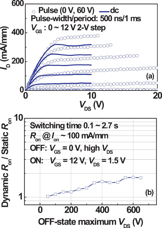
Figure 2: (a) Pulsed drain current versus bias (ID–VDS) characteristics of E-mode MIS-HEMT with LGS = 1μm, (W/L)G = 2x50μm/1μm, and LGD = 10μm. (b) Ratio of dynamic and dc static on-resistance (RON) obtained by low-speed high-voltage switching measurement on device with LGS = 15μm, (W/L)G = 10μm/1μm, and LGD = 15μm.
The current collapse effect seen in HEMTs with pulsed bias was assessed using MIS-HEMTs with 1μm gate-source spacing, 2x50μm gate width, 1μm gate length, and 10μm gate–drain spacing. The devices showed “little difference between the dc and pulsed drain current in the linear region” (Figure 2a). Under pulsed operation, self-heating effects are smaller. The researchers suggest this is the reason for the higher drain current in pulsed-mode compared with dc at larger drain bias.
High-drain-bias stress testing was also carried out (Figure 2b). Below 200V stress, the on-to-off switching time was 0.1 seconds. This increased to 2.7 seconds for higher biases.
http://ieeexplore.ieee.org/xpl/articleDetails.jsp?arnumber=6601638
The author Mike Cooke is a freelance technology journalist who has worked in the semiconductor and advanced technology sectors since 1997.


