


- News
26 November 2013
Limited area epitaxy applied to semipolar GaN laser diodes
University of California Santa Barbara (UCSB) has been using limited area epitaxy (LAE) to improve the performance of lasers diodes (LDs) grown on free-standing semipolar (20-21) gallium nitride (GaN) substrates [Matthew T. Hardy et al, J. Appl. Phys., vol114, p183101, 2013]. The researchers were particularly interested in achieving efficient true green emission. Laser diodes in the green wavelength range (520-570nm) have been difficult to achieve so far.
Laser diode materials grown in semipolar or nonpolar crystal directions should avoid large spontaneous and strain-dependent electric fields arising from differences in polarization of the various layers of the usual polar c-plane (0001) heterostructures. The polarization-dependent electric fields reduce the overlap between electrons and holes, reducing recombination into photons. Reduced recombination results in lower efficiency and higher threshold voltages and currents.
One drawback of epitaxy in semipolar directions is that significant shear stress arises, and slippage in the c-plane can arise in thicker layers of material. This slippage causes misfit dislocations (MDs). The effect is worse when there are pre-existing threading dislocations (TD) arising from the substrate.
LAE performs epitaxy on a series of mesas. This can block the TD glide effects that lead to MDs by preventing the TDs from entering the patterned areas of the mesas.
The UCSB epitaxial material was grown using atmospheric-pressure metal-organic chemical vapor deposition (AP-MOCVD). Mitsubishi Chemical provided the free-standing GaN substrates.
The mesa structures for the LAE were achieved using dry etching. By orienting the mesas along the a-direction of the crystal structure, TD glide can be blocked. Although blocking of TD glide was achieved in some preliminary experiments with an etch depth as small as 250nm, the LDs were produced with 1μm depth “in the interests of process stability”.
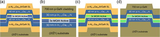
Figure 1: Schematic epitaxial structure for (a) LAE AlGaN-clad blue LD, (b) GaN-clad ‘standard’ blue LD, (c) LAE AlGaN-clad (blue-)green LD and (d) LAE GaN-clad true green LD.
Various blue and green LD structures (Figure 1) were grown to test the effect of using LAE. For the blue LD, a planar device with GaN cladding was also created as a comparison (Figures 1a and 1b).
The use of LAE allowed the creation of modulation-doped AlGaN/GaN short-period superlattice (SPSL) structures as cladding. The n-type cladding was grown on a 600nm n-GaN buffer. The SPSL consisted of 160 periods of 2.5nm/2.5nm layers of alternating material. On the p-side of the device the SPSL was 145 periods of 2.5nm/2.5nm layers.
The active multiple quantum well (MQW) was 3 periods of 3.5nm InGaN separated by 10nm GaN barriers. The waveguide structures consisted of 40nm InGaN on either side of the MQW.
The green LDs (Figures 1c and 1d) were grown using LAE with and without SPSL cladding structures. The MQW InGaN was 2.7nm and the barriers 10nm. The researchers comment: “The quantum wells were thinner to mitigate increased strain and quantum-confined Stark effect in the high-InN-fraction InGaN QWs, and AlGaN barriers were used to suppress dark triangle defects (DTDs).”
The p-type layers for the blue LDs were grown at a lower temperature of 890°C. This temperature is about 60°C lower than normally used by UCSB for blue LDs. The researchers used the lower temperature to simulate the growth conditions often used for producing green LDs.
The LD materials were formed into ridge-waveguide devices aligned to the LAE mesas. Silicon dioxide dielectric was sputtered onto the field and sidewalls of the structures. The p-contacts of palladium/gold were made through self-aligned vias in the dielectric.
The facets for the blue LDs were created by dry etching. The green device facets were achieved through a polishing process. Facet coatings for the green LD consisted of quarter-wavelength layers of silicon dioxide and tantalum pentoxide. The back facet was seven periods, giving estimated 99% reflectivity, and the front two periods (75%).
The blue LD with AlGaN cladding had a threshold current of 4.5kA/cm2, a value “competitive with state-of-the-art blue LDs”. The reduction in threshold is attributed to a significant increase in optical confinement.
The threshold performance of the other devices (Table 1) was less impressive. The researchers say that the extremely high threshold voltage of 23V for the blue-green AlGaN-clad LD “can be attributed to the low AlGaN growth temperature of 890°C and un-optimized p-doping.”
Table 1: Threshold performance of various LDs under pulsed operation.
| Color | Cladding | Ridge | Threshold |
| Blue (456nm) | AlGaN | 2.5x1800μm | 4.5kA/cm2 |
| Blue (456nm) | GaN (planar) | 2.5x1800μm | >8kA/cm2 |
| Blue-green (515nm) | AlGaN | 4x1200μm | 26kA/cm2/23V |
| True green (523.4nm) | GaN | 8x1200μm | 12kA/cm2/15V |
A true green device was achieved using a GaN cladding (Figure 2). The relatively high 15V threshold is again blamed on low-temperature growth of the p-GaN at 840°C.
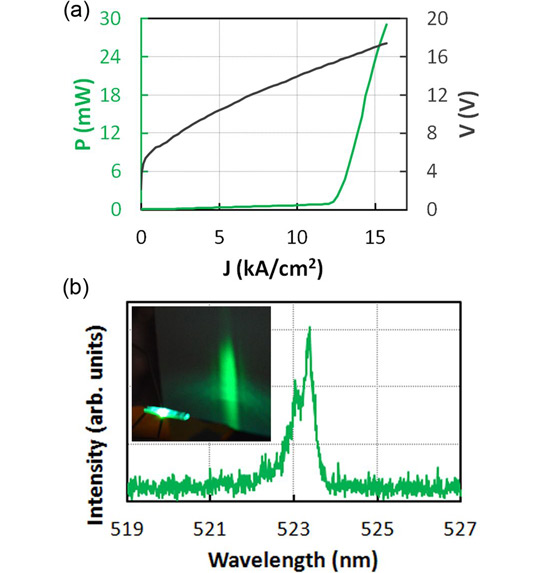
Figure 2: (a) Optical output power and voltage as function of current density for GaN-clad LAE true green LD, and (b) lasing spectra with far-field pattern inset.
The GaN cladding gave a lower optical confinement of 1.9%, compared with 2.5% for AlGaN. However, the use of AlGaN cladding also required the use of AlGaN barriers in the MQW active region to avoid DTDs due to the higher growth temperatures needed. The AlGaN barriers were grown at a very low temperature of 755°C. Such AlGaN is thought to be at risk of oxygen impurity incorporation, which can degrade performance.
The LAE successfully suppressed MD formation in the GaN-clad LD, allowing the use of 65nm InGaN waveguide layers. Without LAE, similarly structured devices are subject to MD formation in waveguide layers thicker than 35nm. The increase from 35nm to 65nm effects an increase in optical confinement from 1.34% to 1.88%.
Green laser diodes GaN laser diodes AP-MOCVD
http://dx.doi.org/10.1063/1.4829699
The author Mike Cooke is a freelance technology journalist who has worked in the semiconductor and advanced technology sectors since 1997.


