


- News
20 November 2013
Electrostatic protection for gallium nitride circuits
Researchers in USA and Taiwan have developed a nitride semiconductor electrostatic discharge (ESD) clamp using gallium nitride (GaN) pseudomorphic high-electron-mobility transistor (pHEMT) technology “for the first time” [Zhixin Wang et al, IEEE Electron Device Letters, published online 10 October 2013]. The researchers are at University of Central Florida and Chang Gung University,
GaN transistor technology is being developed for radio frequency (RF) and microwave applications such as power amplification. Compared with gallium arsenide (GaAs) transistors, the wide bandgap and high critical field allow higher power densities to be achieved in GaN components.
ESD protection is a vital part of development efforts to make GaN a viable and commercial high-frequency and high-power technology. There has been a limited amount of research in this area so far. A recent ESD development in GaAs technology has been a clamp based on pHEMTs. The new research makes a similar development for GaN devices.
“The targeted applications are ESD protection of I/O pins of GaN-pHEMT-based power and low-noise amplifiers used in wireless communication applications with an operating voltage in the range 2–4V,” the researchers write.
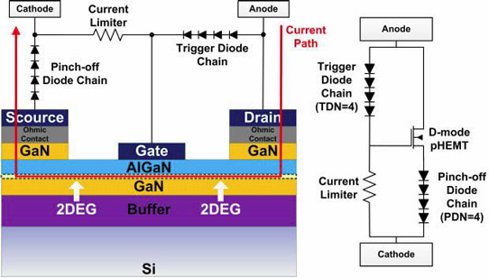
Figure 1: (Left) Cross-sectional diagram of proposed ESD protection clamp, consisting of single-gate depletion-mode GaN pHEMT, trigger diode chain, pinch-off diode chain, and resistor (current limiter). Red line is current path when clamp is on. (Left) Equivalent circuit of GaN-pHEMT-based ESD clamp.
The circuit for the ESD clamp (Figure 1) was laid out (Figure 2) on a substrate that included an aluminium gallium nitride (AlGaN) barrier and gallium nitride (GaN) buffer on silicon. The clamp consisted of a depletion-mode (normally-on) pHEMT with various Schottky diodes to provide trigger and pinch-off diode chains. A current-limiting resistor is also part of the device.
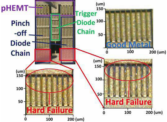
Figure 2: Photograph of GaN pHEMT clamp, with enlarged pictures showing hard failures on pinch-off diode chain.
In a set up with an enhancement-mode (normally-off) pHEMT, the pinch-off chains would not strictly be necessary, in theory. The pinch-off chain also limits the leakage current through the clamp during normal operation when there is no electrostatic charge to dissipate from the core circuit. However, pinch-off diodes increase the on-resistance of the clamp.
The dimensions of the pHEMT device were 188μm x 184μm. The diode dimensions were 106μm x 111μm and 196μm x 169μm for trigger and pinch-off, respectively. The threshold voltage of the pHEMT was -2V. The gate length was 0.35μm.
The clamp was characterized (Table 1) using a transmission line pulsing (TLP) stress tester (Barth 402). The pHEMT-based clamp gives reduced leakage current and on-resistance and higher failure current, compared with structures based just on Schottky diodes. For example, a pHEMT clamp with four trigger and four pinch-off diodes had 2μA leakage and 3A failure currents. A five diode-only clamp of similar area and trigger voltage had ~10μA leakage and ~2A failure currents.
Table 1: Comparisons of trigger voltage, leakage current, on-state resistance, and failure current with different trigger and pinch-off diode numbers.
| Trigger diodes | Pinch-off diodes | Trigger voltage (V) | Leakage current (A) | On-resistance (Ω) | Failure current (A) |
| 2 | 4 | 4.6 | 1.50e-4 | 3.54 to 377 | 2.73 |
| 3 | 4 | 5.2 | 2.23e-5 | 3.42 to 348 | 2.97 |
| 4 | 4 | 6 | 1.93e-6 | 3.36 to 335 | 3 |
| 4 | 3 | 4 | 9.42e-5 | 3.46 to 9.75 | 3.72 |
| 4 | 2 | N/A | >2e-3 | N/A | N/A |
| 4 | 1 | N/A | >2e-3 | N/A | N/A |
The effect of reducing the pinch-off diode number below 3 is that the pHEMT is not fully turned off in normal operation of the core circuit and the leakage is larger than 2mA, far beyond the value needed for applications.
Hard failures occurred in the pinch-off chains (Figure 2). The pHEMT and trigger chains showed no damage. Inspection of the pinch-off diodes showed damage near the anode end of the devices, suggesting problems with non-uniform current crowding. The researchers believe that diodes with larger numbers of shorter fingers could provide a more uniform current and therefore higher robustness for such ESD clamps.
http://ieeexplore.ieee.org/xpl/articleDetails.jsp?arnumber=6627941
The author Mike Cooke is a freelance technology journalist who has worked in the semiconductor and advanced technology sectors since 1997.


