


- News
25 November 2013
First small-signal data from p-channel gallium nitride transistor
RWTH Aachen University has reported the first small-signal response frequency characteristics for p-channel gallium nitride (GaN) heterostructure field-effect transistors (HFETs) [Herwig Hahn et al, Jpn. J. Appl. Phys., vol52, p128001, 2013].
Although the performance of these devices is much inferior to n-channel HFETs, p-channel transistors are of interest for producing GaN-based logic circuits. Complementary logic uses n- and p-channels devices in tandem to give lower power consumption and high switching speed, relative to direct-coupled transistor circuits where only one type of device is used.
For mainstream logic applications, silicon is the material of choice, but GaN-based logic could extend capabilities to harsher environments and higher temperatures. The p-channel HFET side of complementary logic has only intermittently been explored in a GaN setting. RWTH Aachen reported on DC characteristics for a GaN p-HFET earlier this year [H Hahn et al, IEEE Transactions on Electron Devices, vol60, p3005, 2013].
The latest small-signal measurements were on a device grown on 2-inch sapphire using metal-organic chemical vapor deposition (MOCVD) in an Aixtron system (Figure 1). The device layers include a 35nm AlInGaN back-barrier. The positive polarization difference between the back-barrier and underlying 2μm GaN buffer caused a two-dimensional electron gas (2DEG) to form.
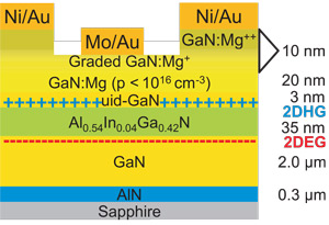 Figure 1: Schematic cross section of double heterostructure field-effect transistor with p-channel.
Above the back-barrier a negative polarization difference caused a two-dimensional hole gas (2DHG) to accumulate in the overlying unintentionally doped (uid) GaN cap. The properties of the hole gas were 2x10¹³/cm2 carrier density, 12cm2/V-s mobility, and 26kΩ/square sheet resistance.
Further epitaxial layers consisted of GaN with varying doping levels of magnesium to create p-type hole conductivity. Ohmic contacts consisted of nickel/gold annealed in an oxygen-rich atmosphere. A ‘digital etch’ was used to create a recess between the source and drain ohmic contacts, removing the highly doped GaN:Mg++ layer to significantly reduce gate leakage. The gate stack consisted of molybdenum/gold. Pads consisting of nickel/gold were applied to all the contacts.
The HFET structure consisted of a double-finger gate of 100μm width and 1μm length. The source-drain and source-gate separations were 2.5μm and 1.5μm, respectively.
The frequency cut-off (fT) and maximum oscillation (fmax) were estimated at 206MHz and 640MHz. “These values are about a factor of 50 lower than the values of n-channel devices fabricated in our group,” the researchers point out.
By measuring fT away from the optimum bias point (Figure 2) and making some assumptions using the transit time and drain current that should be adequate for the relatively large gate length of 1μm, the researchers estimated a hole saturation velocity of 2.4x105cm/s, “which is lower than that of electrons in GaN roughly by a factor of 50–100.”
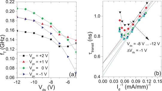
Figure 2: (a) Behavior of fT versus bias points and (b) extracted saturation velocity.
In DC testing, the maximum drain current was -25mA/mm at -3V gate voltage. The threshold voltage was extrapolated at +3.5V. The maximum transconductance was 6mS/mm. While this would be a small value for n-channel HFETs (also known as high-electron-mobility transistors, or HEMTs), it is among the highest reported for p-channel devices.
The researchers foresee improvements via “reducing the gate-channel separation, downscaling the device dimensions, or reducing the parasitic resistances” (e.g. sheet and ohmic contact).
http://jjap.jsap.jp/link?JJAP/52/128001/
The author Mike Cooke is a freelance technology journalist who has worked in the semiconductor and advanced technology sectors since 1997.


