


- News
4 November 2013
Quantum well engineering color-tunable nitride semiconductor LEDs
Chinese Academy of Sciences’ Semiconductor Lighting R&D Center at the Institute of Semiconductors in Beijing has developed an electrically driven color-tunable light-emitting diode (LED) based on indium gallium nitride (InGaN) quantum wells in gallium nitride (GaN) barriers [Hongjian Li et al, Appl. Phys. Express, vol6, p102103, 2013]. At high current injection, the devices achieve a white color rendering index of 85.6 – much higher than for conventional yellow-phosphor converted ‘white’ LEDs.
The color-tunability arises from the nitride semiconductor growth process rather than from complicated device structures or fabrication methods such as adding phosphor layers. The researchers see their development as providing “a simple method for the fabrication of phosphor-free color-tunable monolithic LEDs and also an alternative for high-color-quality general lighting”.
The nitride semiconductor layers (Figure 1) were grown on c-plane sapphire using metal-organic chemical deposition (MOCVD). In detail, the growth sequence was 30nm of GaN nucleation, 2μm of undoped GaN, 2μm of n-type GaN, a 10x InGaN/GaN superlattice ‘underneath layer’, the active multiple quantum well (MQW) stack, a 20nm p-AlGaN electron-blocking layer, and 200nm of p-GaN.
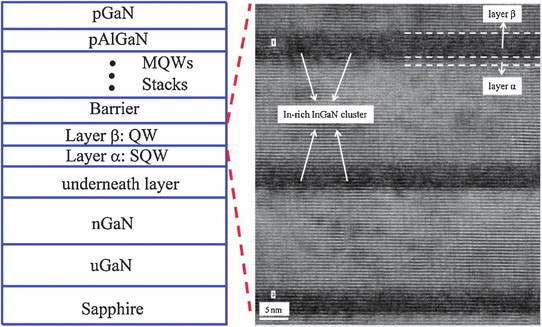
Figure 1: Epitaxial structure (left) and HRTEM image of active region (right).
The quantum wells consisted of a combination of low-indium-content (13%, layer α) InGaN 1nm shallow wells (SQW) and deeper high-indium-content (46%, layer β) InGaN 3nm wells. Barriers between the wells were 17nm of pure GaN. Growth of the α layer before the main β well improved crystal quality, served as a carrier reservoir, and enabled shorter-wavelength emissions.
A high-resolution transmission electron micrography (HRTEM) study showed indium-rich InGaN clusters of 2-4nm diameter embedded in the deep quantum well regions. The researchers attribute the clusters to strong indium phase separation and composition fluctuations due to the large biaxial strain from the large lattice mismatch between InN and GaN (11%). The In-rich clusters in high-indium-content InGaN result in deep localization centers for carrier recombination. Clusters are a common feature of high-indium-content (more than 20% In) InGaN.
Photoluminescence showed peaks at 2.12eV (P1) and 2.91eV (P2). The P1 peak is attributed to the shallow well, while P2 correlates with the deep well. Temperature-dependent measurements suggested internal quantum efficiencies of 10.4% and 14.1% for P1 and P2, respectively.
Standard mesa-type LEDs of 500μm x 1000μm size were produced with an indium tin oxide (ITO) transparent conductor current spreader on the p-contact layer. The contact electrodes were chromium/platinum/gold.
The LEDs were fixed on an aluminium thermally conducting substrate for electroluminescence (EL) measurements. The spectral content of the emission shifted significantly with increasing current from red (5mA) through yellow (10-20mA) to ‘white’ (100mA). The researchers comment: “This varied emission color versus injection current suggests a good electrically driven color-tunable characteristic, without introducing any phosphor.”
The turn-on voltage of the device was 2V and the forward voltage at 100mA was 3.06V. The spectra of the emissions showed a dominant red (631nm) peak at 5mA. This peak blue shifted to 615nm and 608nm at 10mA and 20mA, respectively. The width of the peak broadens from a full-width at half-maximum (FWHM) of 185meV at 5mA to 274meV at 60mA. The broadening is attributed to filling of the deeper localization states as the current increases, which allows shallower localization states to become active. Above 60mA, a second peak appears at 473nm, attributed to the shallow well.
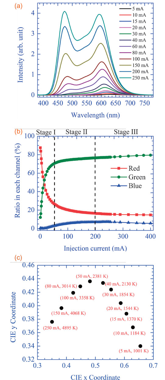
Figure 2: (a) EL spectra at various injection currents. (b) Intensity ratio in red/green/blue channels versus injection current. (c) CIE chromaticity coordinates at various injection currents.
The researchers plotted Commission International de I’Éclairage (CIE) chromaticity coordinates and determined the color temperature at the various currents (Figure 2). The color rendering index (CRI) at 250mA was 85.6. The researchers point out that this is much higher than CRI values obtained for conventional yellow-phosphor-converted white LEDs.
Phosphor-free monolithic white LEDs InGaN quantum wells MOCVD
http://apex.jsap.jp/link?APEX/6/102103
The author Mike Cooke is a freelance technology journalist who has worked in the semiconductor and advanced technology sectors since 1997.


