

- News
22 May 2013
NCSU develops new technique for atomic-layer thin-film growth
Funded by the US Army Research Office, researchers at North Carolina State University (NCSU) have developed a new technique for creating high-quality semiconductor thin films at the atomic scale (just one atom thick). The technique can be used to create the thin films on a large scale, sufficient to coat wafers that are 2-inches wide, or larger.
“This could be used to scale current semiconductor technologies down to the atomic scale – lasers, light-emitting diodes (LEDs), computer chips, anything,” says Dr Linyou Cao, an assistant professor of materials science and engineering at NC State and senior author of the paper ‘Controlled Scalable Synthesis of Uniform, High-Quality Monolayer and Few-layer MoS2 Films’ published online in Scientific Reports (a journal of the Nature Publishing Group). “People have been talking about this concept for a long time, but it wasn’t possible. With this discovery, I think it’s possible,” he adds.
The researchers worked with molybdenum sulfide (MoS2), an inexpensive semiconductor material with electronic and optical properties similar to materials already used in the semiconductor industry. However, MoS2 can be grown in layers just one atom thick without compromising its properties.
 Picture:
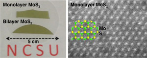
As-grown MoS2 monolayer (1L) and bilayer (2L) films (left); high-angle annular dark-field (HAADF) scanning transmission electron microscopy (STEM) image of MoS2 monolayer film (right).
Picture:
As-grown MoS2 monolayer (1L) and bilayer (2L) films (left); high-angle annular dark-field (HAADF) scanning transmission electron microscopy (STEM) image of MoS2 monolayer film (right).
In the new technique, researchers place sulfur and molybdenum chloride powders in a furnace and gradually raise the temperature to 850°C, which vaporizes the powder. The two substances react at high temperatures to form MoS2. While still at high temperature, the vapor is then deposited in a thin layer onto the substrate.
“The key to our success is the development of a new growth mechanism, a self-limiting growth,” Cao says. The researchers can precisely control the thickness of the MoS2 layer by controlling both the partial pressure (the tendency of atoms or molecules suspended in air to condense into a solid and settle onto the substrate) and the vapor pressure (the tendency of solid atoms or molecules on the substrate to vaporize and rise into the air) in the furnace.
To create a single layer of MoS2 on the substrate, the partial pressure must be higher than the vapor pressure. The higher the partial pressure, the more layers of MoS2 will settle to the bottom. If the partial pressure is higher than the vapor pressure of a single layer of atoms on the substrate, but not higher than the vapor pressure of two layers, then the balance between the partial pressure and the vapor pressure can ensure that thin-film growth automatically stops once the monolayer is formed. Cao calls this ‘self-limiting’ growth.
Partial pressure is controlled by adjusting the amount of molybdenum chloride in the furnace – the more molybdenum is in the furnace, the higher the partial pressure. “Using this technique, we can create wafer-scale MoS2 monolayer thin films, one atom thick, every time,” Cao says. “We can also produce layers that are two, three or four atoms thick.”
Cao’s team is now trying to find ways to create similar thin films in which each atomic layer is made of a different material. Cao is also working to create field-effect transistors (FETs) and LEDs using the technique. He has filed a patent on the new technique.
www.nature.com/srep/2013/130521/srep01866/full/srep01866.html
www.mse.ncsu.edu/research/linyou
