

- News
28 May 2013
LayTec’s EpiCurveTriple TT used for 200mm GaN-on-Si at Singapore’s IMRE
LayTec AG of Berlin, Germany (which makes in-situ metrology systems for thin-film processes, focusing on compound semiconductor and photovoltaic applications) says that, in his invited talk at the LED Technology Forum in Singapore (7-10 May), Dr Sudhiranjan Tripathy of IMRE (Institute of Materials and Research Engineering) - part of Singapore’s Agency for Science, Technology and Research (A*STAR) - revealed the latest results of gallium nitride (GaN) growth on 200mm-diameter silicon substrates. His team uses LayTec’s in-situ monitoring system EpiCurveTriple TT in the development of epiwafers for InGaN/GaN light-emitting diodes (LEDs) and GaN power electronic devices.
LayTec says that the EpiCurveTriple TT is suited to 200mm real-time wafer characterization due to of its three sensor heads for radial analysis ofgrowth conditions. It provides wafer bow and temperature measurements, as well as simultaneous detection of growth rate and surface morphology.
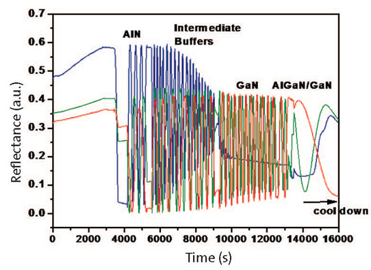
Figure 1: Reflectance monitoring of AlGaN/GaN HEMT structure grown on 1mm-thick 200mm diameter Si(111) at IMRE: blue - 405nm, green - 633nm, red - 950nm.
Figure 1 shows reflectance profiles at three wavelengths: 950nm for emissivity correction of pyrometry, 633nm for analysis of thick layers (e.g. GaN buffer), and 405nm for thin layers. Figure 2 demonstrates how the 405nm reflectance is used for individual in-situ tuning of each well and barrier within the multi-quantum-well stack. The in-situ signal (Figure 2 - left) corresponds with the multi-quantum wells (MQWs), as can be seen in the scanning transmission electron microscopy (sTEM, Figure 2 - right).
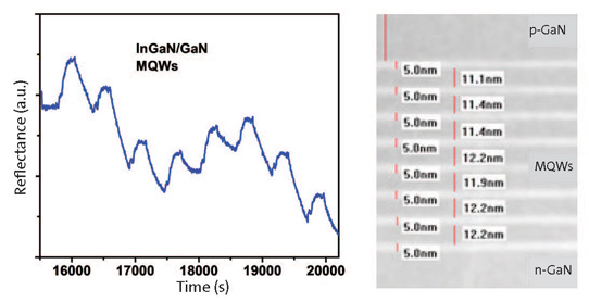
Figure 2: 405nm reflectance (left) of InGaN/GaN MQW stacks and corresponding sTEM image of the MQWs (right).
According to Tripathy’s team, LayTec’s in-situ metrology is a key element for identifying the epitaxial process optimization potentials. In comparison to the time-consuming, destructive ex-situ cross-section transmission electron microscopy (TEM) analysis, the in-situ tool provides real-time information on growth thickness and homogeneity during growth. LayTec says that its system has significantly reduced IMRE’s R&D cycles for epitaxial growth optimization and enables faster industrialization of GaN-on-silicon (GaN-on-Si) technology.
