

- News
16 May 2013
Fast growth of graphene for nitride LED transparent contacts
Researchers based in China and Sweden have proposed fast chemical vapor deposition (CVD) of graphene as a route to more cost-effective transparent conducting layers (TCLs) for nitride semiconductor light-emitting diodes (LEDs) [Xu Kun et al, Appl. Phys. Lett., vol102, p162102, 2013]. The research involved China’s Key Laboratory of Optoelectronics Technology (Beijing University of Technology) and Sweden’s Chalmers Tekniska Högskola AB.
There has been much interest recently in using graphene as a component of TCL structures for nitride LEDs. One problem is that fabrication of high-quality single-crystal graphene can take many hours. By contrast, the proposed polycrystalline graphene is grown in half an hour. Despite its polycrystalline nature, the resulting graphene is found to have conductivity similar to that of normal graphene prepared by more laborious methods.
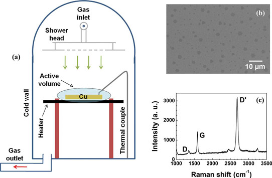
Figure 1: (a) Schematic of cold-wall CVD. Gases are injected from shower head over sample on heater. Active hot volume is very small compared with hot-wall systems. (b) SEM image of high-density graphene nucleation during early-stage deposition on liquid Cu, captured after cooling to room temperature. (c) Typical Raman spectrum of graphene. D’ peak intensity is more than twice as high as G peak. Small D peak indicates the high quality of film.
The fast graphene was grown on polycrystalline copper in a cold-wall Aixtron CVD system (Figure 1). The substrate was first cleaned, then heated to 1000°C at 300°C/min and annealed for 5 minutes. The graphene source was methane (CH4) in hydrogen/argon. The growth step was only 5 minutes. The sample was quench-cooled by shutting off the heater. The researchers see the fast growth rate as being related to the small active region with a high concentration of reactants near the deposition site enabled by the use of a cold-wall system.
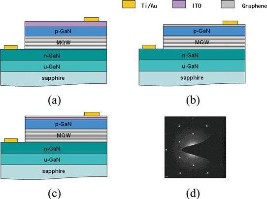
Figure 2: LED structures with various TCLs: (a) type I (240nm ITO), (b) type II (3-layer graphene), and (c) types III, IV and V (3, 7 and 10 nm ITO+3-layer graphene). MQW denotes multiple quantum wells. (d) Typical selected-area electron diffraction pattern of graphene. Six-fold symmetric dots with equal intensity strength indicate high-quality monolayer graphene.
The epitaxial structure for the LED (Figure 2) was a commercial product grown on c-plane sapphire. The material was fabricated into mesa-structure LEDs with different transparent conducting layer structures. Indium tin oxide (ITO) layers were produced using electron-beam evaporation.
The graphene was transferred to the ITO surface by spin coating a poly(methyl methacrylate) (PMMA) mechanical support layer and etching away the copper foil in ferric chloride (FeCl3) solution.
The mesa structures were defined by photolithography and plasma etching of graphene, ITO and nitride semiconductor. The metal electrodes consisted of titanium/gold.
Monolayer graphene as-deposited had a sheet resistance range of 800-1000Ω/square. Increasing the number of layers to three reduced the range to 300-350Ω/square. The mobility was around 2000cm2/V-s. The sheet resistance values are similar to those achieved for standard graphene.
Optical inspection of the light emission at 20mA shows that the devices with graphene emit more uniformly across the device, indicating successful current spreading. By contrast, a 10nm ITO-only TCL LED emits more brightly closer to the p-electrode.
Graphene-only TCLs suffer from a large work-function mismatch with the p-GaN layer. The mismatch results in a high 6.76V forward voltage needed to drive 20mA current through a 3-layer graphene device. High forward voltage means power losses and hence lower efficiency. By inserting a thin 7nm ITO layer the forward voltage was reduced to 3.90V. An LED with a 240nm ITO layer had a forward voltage at 20mA of 3.6V.
An alternative technique to bring the graphene work-function closer to that of p-GaN is doping. However, the known techniques for this are not stable over time. Another way forward may be to grow carbon films directly on p-GaN. Adhesion of graphene is generally better to GaN than GaAs, due to a closer lattice affinity. Chalmers researchers recently reported a technique for direct growth on p-GaN that resulted in a carbon film with “optical transparencies comparable to that of exfoliated graphene” [Jie Sun et al, IEEE Transactions on Semiconductor Manufacturing, vol25, p494, 2012].
In terms of optical transmission, although the 10nm ITO+3-layer graphene and 240nm ITO TCLs perform comparably at long wavelengths, at ultraviolet wavelengths of 320nm the former transmits 78.6% and the latter 58.9%.
http://link.aip.org/link/doi/10.1063/1.4802798
The author Mike Cooke is a freelance technology journalist who has worked in the semiconductor and advanced technology sectors since 1997.
