

- News
3 May 2013
CrystAl-N switches to 2-inch bulk AlN wafer production
 AlN crystal maker CrystAl-N GmbH of Fürth, Germany says it is now moving from production of 1-inch to 2-inch AlN and accepting pre-orders. According to the firm, which was founded in 2010 as spin-off of Friedrich-Alexander-University Erlangen-Nuremberg, AlN will boost the efficiency of deep UV LEDs, lasers and high-power, high-frequency devices as soon as its cost-performance ratio is competitive. Shifting production to larger substrates will help realize this.
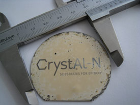
Figure 1: 2-inch wafer.
“After many years of R&D we finally managed to combine high uv transparency with suitable wafer size enabling a real commercial product,” said CTO Boris Epelbaum. “Further diameter increase in our patented tungsten based furnaces is not limited as we are using SiC as initial seed.”
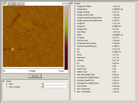
Figurec 2: AFM image (1 x 1 μm2) of a polished c-plane wafer. Ra surface roughness < 0.3 nm
Besides diameter enlargement wafer polishing drastically improved as well. “The corresponding wafers feature surface roughness of less than 0.3 nm and are highly UV transparent”, added Octavian Filip, Director of Wafering.
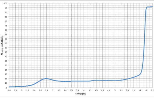
Figure 3: Low absorption coefficient values up to the band edge (peak at 2.8 eV - reason for yellowish coloration of bulk AlN grown by PVT).
