

- News
19 March 2013
Bringing photoelectrochemistry and catalysis to bear on GaN planarization
Researchers in Japan have been developing planarization techniques for gallium nitride (GaN) surfaces [Shun Sadakuni et al, Jpn. J. Appl. Phys., vol52, p036504, 2013]. The researchers from Osaka University, Ritsumeikan University and Ebara Corp are interested in enabling growth of single-crystal GaN with low dislocation densities using methods such as hydride vapor phase epitaxy (HVPE), ammonothermal and sodium-flux techniques. These processes need atomically flat GaN surfaces to promote high-quality, low-defect growth.
The team has been developing photoelectrochemical etch techniques for some time that involve ultraviolet (UV) illumination. In the latest work, the researchers have explored the additional use of electrical biasing, along with a catalyst plate that creates local acidity to cause removal to occur only at protruding regions of the wafer surface. Although the root-mean-square (RMS) roughness of the plate is 0.5μm, the resulting roughness of the GaN wafer is much less due to rotation averaging out the removal rate.
The purpose of the UV illumination is to generate carriers (electron-hole pairs) that encourage oxidation and etching of the GaN surface. However, the effect of the UV tends to be quickly saturated due to the recombination of carriers at defects. This results in a rough surface. By applying the bias, the carriers are separated and hence are less likely to recombine (Figure 1).
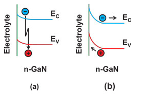 Figure 1: Surface energy band diagram for n-GaN: (a) without an external bias, photo-induced carriers are depleted; (b) the carriers separate when a positive bias is applied, resulting in effective oxidation.
The researchers processed a commercial 2-inch free-standing n-type GaN(0001) wafer with a carrier concentration of 1-3x10¹⁸/cm3. The surface was first polished mechanically using a diamond slurry with particle sizes of ~1μm.
The researchers then investigated etching and planarization processes under UV illumination and electrical biasing. The planarization system uses a grooved silica glass catalyst plate (Figure 2). The wafer and catalyst plate were independently rotated. The pressure between the wafer and catalyst plate was 400hPa. The process was performed in a neutral buffer solution containing 25 millimole/liter (mM) monopotassium phosphate (KH2PO4) and 25mM disodium hydrogen phosphate (Na2HPO4) (pH 6.9). The aim of the buffer is to prevent isotropic dissolution of the oxide. Silanol groups (Si-OH) at the surface of the silica glass donate protons to create local acidity. The 4mW/cm2 UV radiation was transmitted through the transparent plate and wafer.
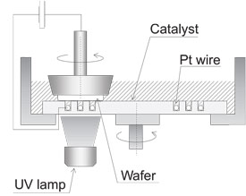 Figure 2: Schematic diagram of planarization apparatus. Pt wires, which act as cathode, are set in grooves of catalyst plate. The GaN surface is illuminated by UV light through transparent catalyst.
The bias was applied to platinum wires in the 1mm-deep plate grooves as cathode and the wafer surface was the anode. The gap between grooves was 3mm.
In the planarization process, the application of a 1V bias produced a removal rate of 60nm/hour. A similar removal rate was seen after 30 hours without the bias, but there is then a long period of increase in removal beginning at 0nm/hour.
With the bias applied, the RMS roughness was reduced to 2.2nm from 3.3nm (Figure 3a). Scratches from the mechanical polishing step are removed, but stripe patterns from the crystal growth process appear.
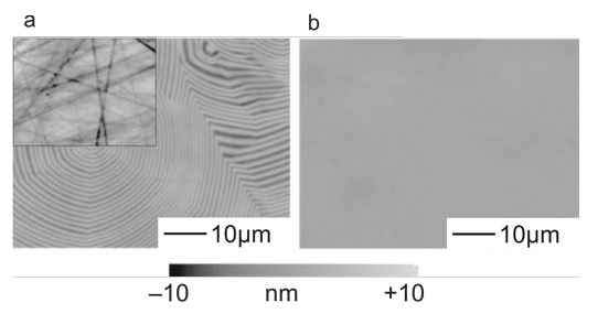
Figure 3: Optical interferometric images (71μm x 53μm) of (a) processed surface with applied voltage of 1V and (b) surface processed without applying a voltage. The inset shows an unprocessed surface.
The stripe patterns were blamed on the solution near the GaN surface becoming excessively acidic due to anodic reactions with positive bias. “The acidic solution removes the oxide even from areas that did not contact the catalyst plate,” the researchers write.
A second planarization step without bias for 30 minutes was found to reduce the RMS roughness to 0.3nm (Figure 3b).
As a preliminary to the planarization work, the researchers also studied an etch process that used a 10mW/cm2 mercury-xenon lamp and 0.01M-concentration potassium hydroxide solution. An electrical bias was applied through a platinum foil cathode in the solution with the wafer surface acting as anode. The etch process removed scratches from the mechanical polishing, but created stripe patterns from the crystal growth process.
http://jjap.jsap.jp/link?JJAP/52/036504
The author Mike Cooke is a freelance technology journalist who has worked in the semiconductor and advanced technology sectors since 1997.
